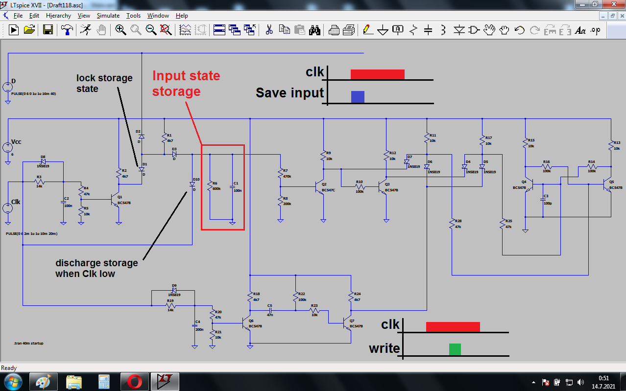
I am trying to make a low speed D flip-flop (positive edge triggered) with idea to save D input state into 100n capacitor, lock it, wait few ms and finally write state to output bistable circuit. It is working fine but run into a problem how to isolate a C1 capacitor charge. A D10 diode serves for quick discharging of C1 after Clk becomes low. When I use as D10 a schottky diode the leakage causes an unwanted C1 charging from Clk signal. Can this be an isssue in real design or it is just a schottky diode simulation inaccuracy?
-
\$\begingroup\$ "can this be an issue in real design"...why do you think your design is the same as an actual production flip-flop that used BJTs? Did you copy the design of a 7474 or something? \$\endgroup\$– Elliot AldersonCommented Jul 13, 2021 at 23:36
-
\$\begingroup\$ @Elliot Alderson I did copy no design, it is whole just my idea. Im curious if the schottkys can have so huge leackage to charge 100n in few ms. \$\endgroup\$– user208862Commented Jul 13, 2021 at 23:47
-
1\$\begingroup\$ Now I found it couses 1N5819 only (probably power type of diode) what makes a leakage about 20uA, I tried a signal schottky what deacresed leakage to negligible level so it is working fine now. \$\endgroup\$– user208862Commented Jul 14, 2021 at 0:47
-
\$\begingroup\$ @MichalP Is this a start sampling on rising edge, and continue sampling for delay #1 after which point the input no longer can influence the sample, followed by an analog-to-digital conversion of the analog sample being held, whose conversion after delay #2 is to be transferred to a bistable latch mechanism? I'm not sure and I'm not going to read that schematic to suss it out, either. (Holding the analog value for long periods is going to be fun.) \$\endgroup\$– jonkCommented Jul 14, 2021 at 7:06
-
\$\begingroup\$ What a bizarre mix of technology! You already have a proper DTL NAND gate (e.g., D6, D7, R11, R28, Q5 and R13 -- more inputs just requires more diodes). You can use this as a building block for more complex circuits. A true edge-triggered DFF can be constructed from six 3-input NAND gates, with no need for odd internal timing circuits or dynamic storage of data in capacitors. \$\endgroup\$– Dave TweedCommented Jul 14, 2021 at 11:16
1 Answer
The whole circuit is awful. You have 400nF of capacitance across the clock input through the diodes. A real clock source won't like this. The circuit is also more complex than it needs to be.
But to answer your question, yes it can be an issue in a real design. The diode you chose appears to have a simulated reverse leakage current of ~30 μA. This may be higher than its typical real-world value at 25 °C, but leakage increases exponentially with temperature so a higher simulated value may be more realistic when the diode is used in a typical (high power) application.
For low leakage you should chose a signal diode such as BAT54 (~60 nA leakage at -5 V and 25 °C) or 1N4148 (~10 nA).
-
\$\begingroup\$ Clk is driven from NPN with 100k base resistor so the discharge current should be in safe level (with Beta=150 about 8mA). I can add a series resistance to diodes if I decide its necessary, for now I try to make it simple. Thx for informations about leakage. Where do you see a complexicity? \$\endgroup\$– user208862Commented Jul 14, 2021 at 5:59


