I'm studying digital circuits and I have a question about the propagation delay of a logic gates. I've read that propagation delay is defined as the time required for the output to reach 50% of its final output level from when the input changes to 50% of its final input level. But what means to "reach 50%" of a logic value like 1 or 0? I know that each logic values are represented through different voltage level, but for me is still difficult to understand the concept of "50%". 50% of what?
-
1\$\begingroup\$ Of voltage level which means 1.. Fx f you have 5v gate then upper 2.5v means true and low 2.5v mean false (not whole true since this depends on gate itself and you may find high/low levels in datasheet) \$\endgroup\$– SelvinCommented Apr 7, 2022 at 8:30
2 Answers
It's important to always remember that digital electronics is just 'convenient analogue' electronics.
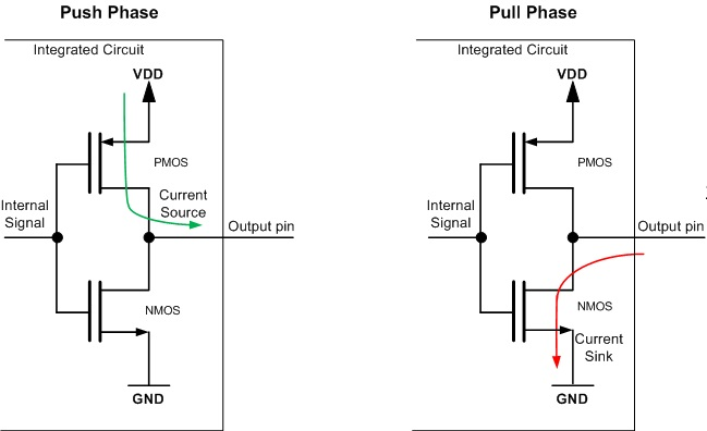
The logic input stage and logic output stage are made from transistors, as shown below. As such, they have switching time that gives the stage a transition (change) time.
When a logic output goes from driving LOW to driving HIGH ('push phase' in diagram), that output waveform will have a rise time. How fast that is depends on the driver itself and the load on it: PCB track/pin capacitances that need charging, loading current etc. The more it's loaded, the slower the rise time.
Similarly, when going from HIGH to LOW ('pull phase' in diagram), the output will have a fall time. Those same load capacitances needs discharging and a loading current will need sinking.
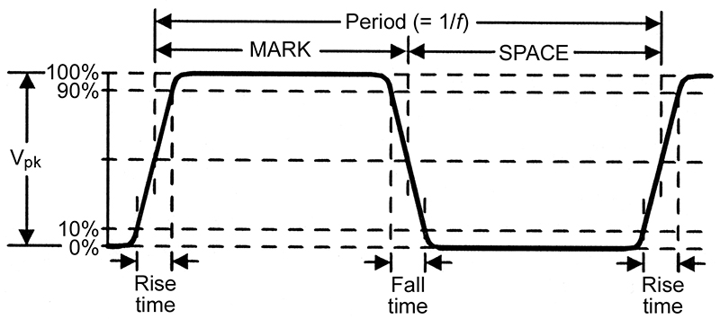
So the transitions are measured from specific voltage points along those rise times and fall times. Here, your 50% refers to when a logic output crosses the 50% of its gate supply voltage, on the way up when rising or the way down when falling. See the waveform diagram below.
-
\$\begingroup\$ Thank you for the expanation, it's very useful. Only one thing: the current shown in the image above, in particular the current that flows through the PMOS transistor, it is a current whose effect is to charge parasitic capacitance, right? It is not a current that flows to other logic gates. \$\endgroup\$– BenderCommented Apr 7, 2022 at 11:59
-
\$\begingroup\$ @Bender, that's covered in the answer. The output high load current flows into whatever the gate is loaded with - that depends on what it's connected to. The output sink current comes from that same load. If it's just other gates then the load is the input leakage currents of those gates. The gates don't draw 0 A, as you can see in their datasheets. \$\endgroup\$– TonyMCommented Apr 7, 2022 at 12:20
The 50% you refer to is the mid point of the two voltages that define the 0 and 1 states.
This is because what is being described is a measurement, and it's convenient to measure to well-defined and fast-changing points on the voltage waveform.
Strictly speaking, we should not use the propagation delay figures defined in this way for the design of logic circuits on its own. It takes longer than the propagation delay for the output of a gate to reach a valid logic level.
However, we do use propagation delay when designing with pencil and paper, and that's generally satisfactory for several reasons.
- the propagation delay measurement starts from 50% as well, and the offset to valid logic levels tends to cancel out at both ends
- when we design with 'worst case' timing figures, a lot of slack is built in for capacitive loading, and worst case voltage and process variations, so there's always a bit of timing contingency in hand (some people design with 'typical' figures and tend to get away with it, but it's usually on the day of the big demo to the VIPs that the timing bites their system (now how would I know that?))


