0
\$\begingroup\$

I am trying to understand working principles of attached class C inductance loaded power amplifier: enter image description here
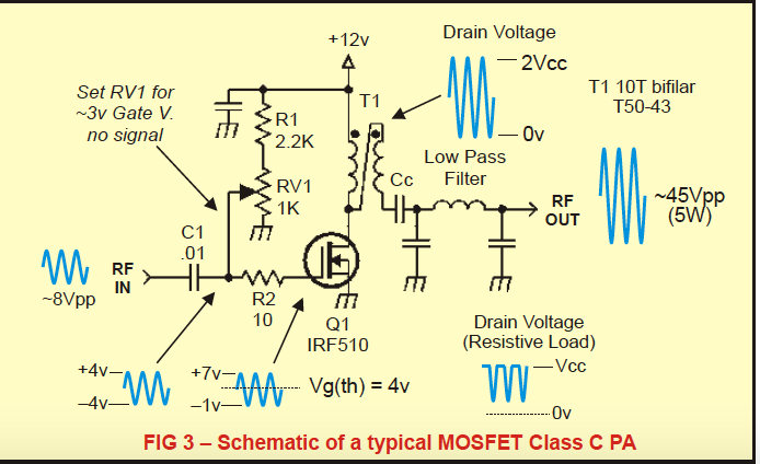
Can you please explain how is it possible that RF OUT pp voltage is almost equal to 4Vcc?

See article by Paul NA5N "The handiman's guide to MOSFET Switched Mode Amplifiers" https://hyse.org/pdf/www.aoc.nrao.edu/~pharden/hobby/_ClassDEF1.pdf for partial explanation. I can understand why drain voltage reaches 2Vcc, but how bifilar 10T transformer can increase it further by almost factor of 2 is a mistery.

\$\endgroup\$

1 Answer 1

2
\$\begingroup\$

I can understand why drain voltage reaches 2Vcc, but how bifilar 10T transformer can increase it further by almost factor of 2 is a mystery.

Because the transformer secondary connects to the primary at the MOSFET drain and, because the secondary has an induced voltage across its terminals of almost twice Vcc, the final secondary voltage feeding the coupling capacitor is double what is induced across the secondary.

Consider if the secondary was connected to GND instead of the MOSFET drain; it would only act as a 1:1 device but, because the secondary is connected to the drain you get double the voltage when the secondary dots are shown as per your image.

In other words the AC voltage on the MOSFET drain is bootstrapping the secondary induced voltage.

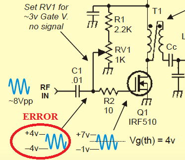
Incidentally, there is a waveform amplitude error in that diagram: -

enter image description here

Clearly the AC voltage after the C1 capacitor is subject to the same DC bias as that on the gate.


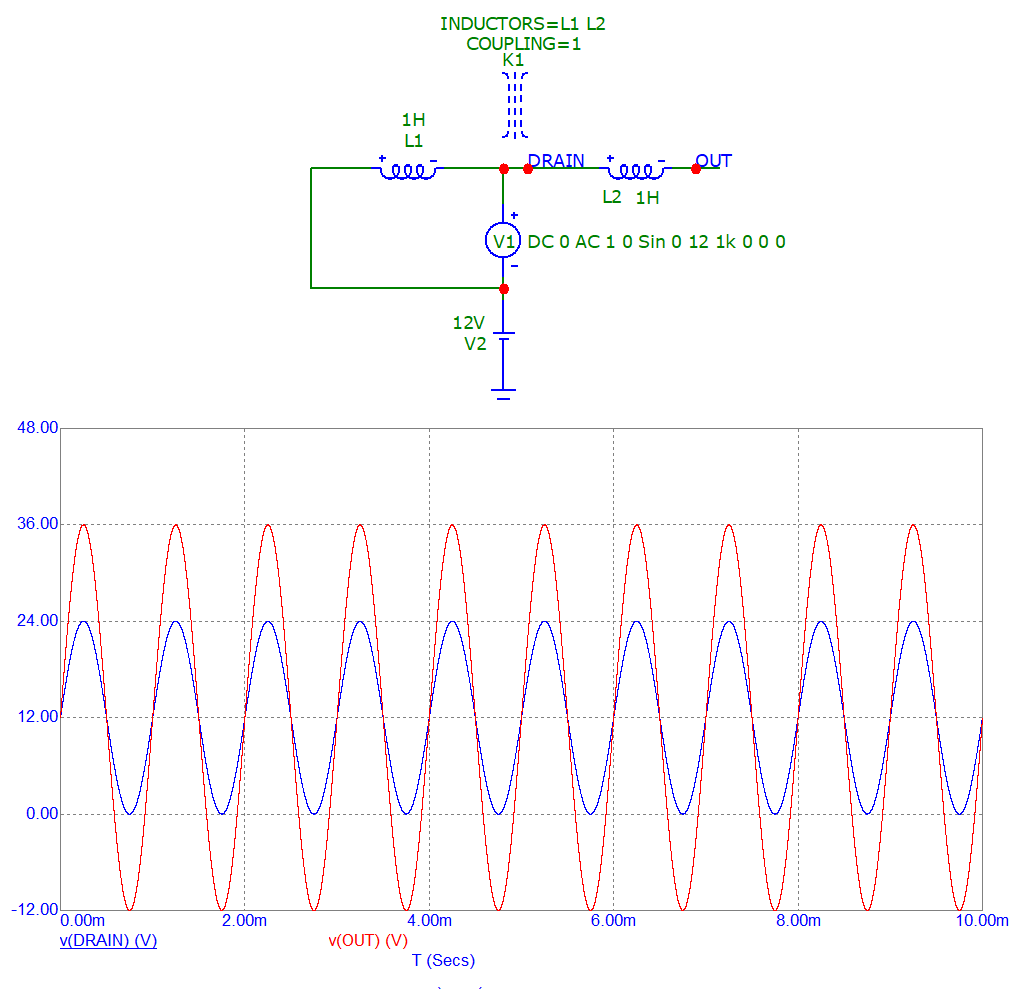
Simulation added: -

enter image description here

\$\endgroup\$
9
  • \$\begingroup\$ Thank you for quick response Andy, so in depicted configuration transformer is 1:2? Could you please support your answer with some formulas? \$\endgroup\$
    – andrzej
    Commented May 5 at 14:14
  • \$\begingroup\$ The transformer is not 1:2; it's 1:1 but, the secondary is bootstrapped by the drain voltage and this doubles the output voltage feeding Cc. Formulas won't help here. It's all about seeing it. \$\endgroup\$
    – Andy aka
    Commented May 5 at 14:37
  • \$\begingroup\$ @andrzej I've added a simulation to show the waveforms. Note that both inductors are the same value, the coupling between them is unity and, I've used 1 kHz arbitrarily. \$\endgroup\$
    – Andy aka
    Commented May 5 at 14:48
  • \$\begingroup\$ Hi Andy, why did you chose not to connect one of the ac source terminals directly to ground so both ac and dc sources have one terminal grounded. \$\endgroup\$
    – andrzej
    Commented May 5 at 18:29
  • \$\begingroup\$ I put them in series to create the blue waveform that has peaks of 0 volts and 24 volts, just as you would get from your MOSFET circuit @andrzej \$\endgroup\$
    – Andy aka
    Commented May 5 at 18:32

Your Answer

By clicking “Post Your Answer”, you agree to our terms of service and acknowledge you have read our privacy policy.

Not the answer you're looking for? Browse other questions tagged or ask your own question.