3
\$\begingroup\$

enter image description here

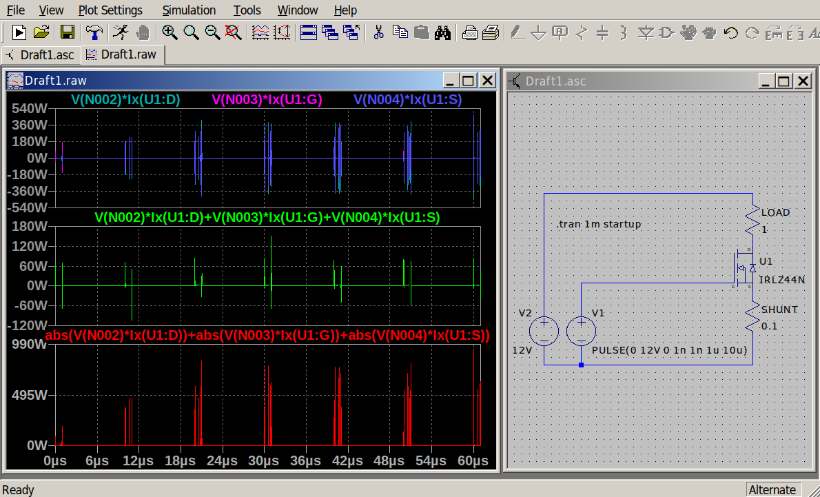
When I Alt-click on the mosfet U1, the green graph is shown. Ctrl-click on the green formula shows an average dissipation of 279.46mW

The formula in red is changed, I wanted absolute values for the three parts that are summed. Ctrl-click on the red formula shows an average dissipation of 605.6mW

A rather large difference. Is there an error in LTspice, the mosfet model or is my assumption incorrect that I need to sum absolute values?

I've seen this negative dissipation issue before in other mosfets but i've added the model below just in case.

.SUBCKT irlz44n 1 2 3
**************************************
*      Model Generated by MODPEX     *
*Copyright(c) Symmetry Design Systems*
*         All Rights Reserved        *
*    UNPUBLISHED LICENSED SOFTWARE   *
*   Contains Proprietary Information *
*      Which is The Property of      *
*     SYMMETRY OR ITS LICENSORS      *
*Commercial Use or Resale Restricted *
*   by Symmetry License Agreement    *
**************************************
* Model generated on Apr 24, 96
* Model format: SPICE3
* Symmetry POWER MOS Model (Version 1.0)
* External Node Designations
* Node 1 -> Drain
* Node 2 -> Gate
* Node 3 -> Source
M1 9 7 8 8 MM L=100u W=100u
* Default values used in MM:
* The voltage-dependent capacitances are
* not included. Other default values are:
*   RS=0 RD=0 LD=0 CBD=0 CBS=0 CGBO=0
.MODEL MM NMOS LEVEL=1 IS=1e-32
+VTO=2.08819 LAMBDA=0.0038193 KP=67.9211
+CGSO=1.59143e-05 CGDO=3.04562e-08
RS 8 3 0.014066
D1 3 1 MD
.MODEL MD D IS=4.4574e-09 RS=0.007275 N=1.40246 BV=55
+IBV=0.00025 EG=1.14011 XTI=3.00078 TT=0
+CJO=8.92434e-10 VJ=4.94724 M=0.75496 FC=0.5
RDS 3 1 2.2e+06
RD 9 1 0.00179971
RG 2 7 2.4114
D2 4 5 MD1
* Default values used in MD1:
*   RS=0 EG=1.11 XTI=3.0 TT=0
*   BV=infinite IBV=1mA
.MODEL MD1 D IS=1e-32 N=50
+CJO=1.15401e-09 VJ=0.859156 M=0.642548 FC=1e-08
D3 0 5 MD2
* Default values used in MD2:
*   EG=1.11 XTI=3.0 TT=0 CJO=0
*   BV=infinite IBV=1mA
.MODEL MD2 D IS=1e-10 N=0.4 RS=3e-06
RL 5 10 1
FI2 7 9 VFI2 -1
VFI2 4 0 0
EV16 10 0 9 7 1
CAP 11 10 3.64838e-09
FI1 7 9 VFI1 -1
VFI1 11 6 0
RCAP 6 10 1
D4 0 6 MD3
* Default values used in MD3:
*   EG=1.11 XTI=3.0 TT=0 CJO=0
*   RS=0 BV=infinite IBV=1mA
.MODEL MD3 D IS=1e-10 N=0.4
.ENDS

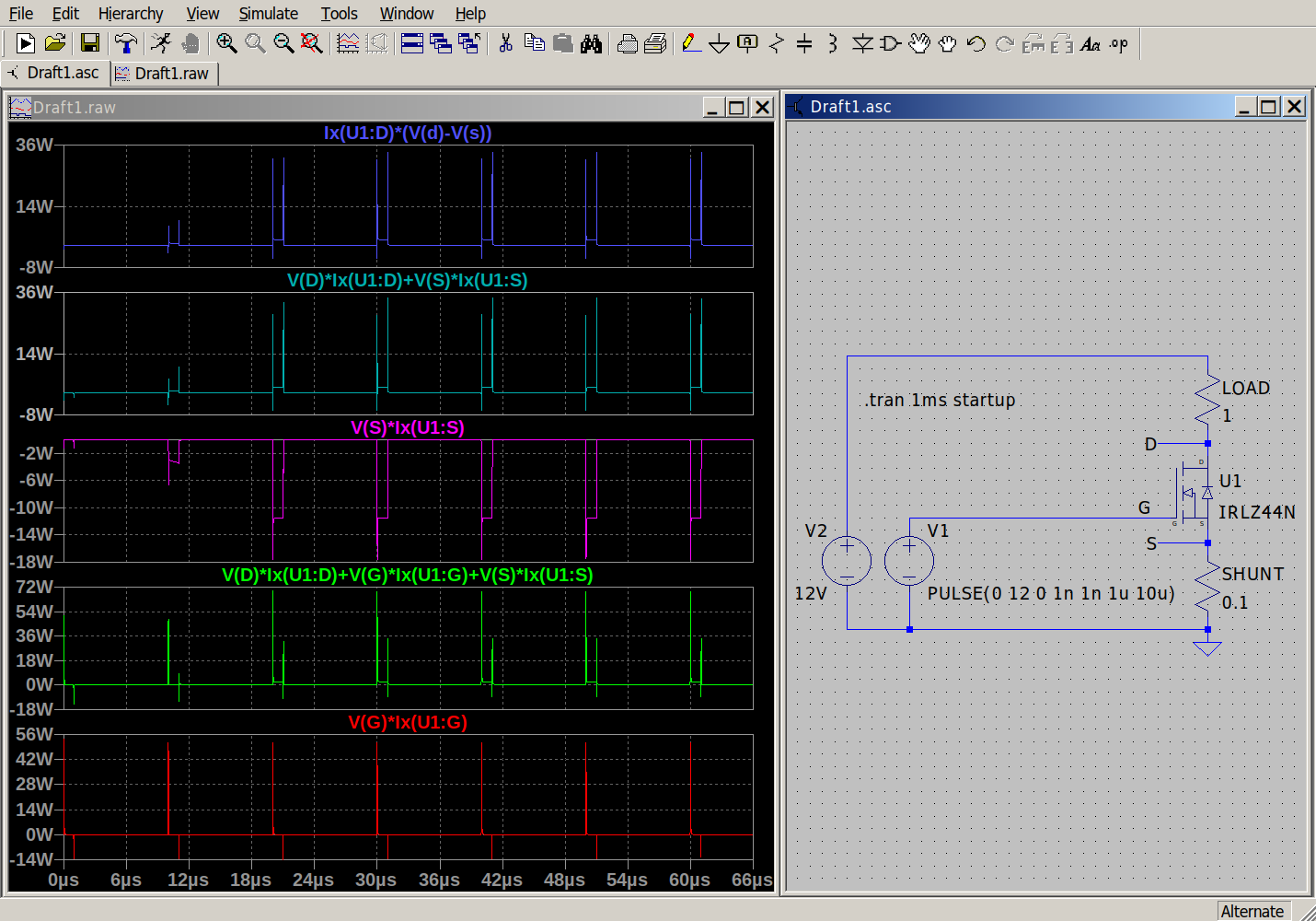
UPDATE: I forgot the ground connection, and that explains the odd 360W spikes in the above circuit. enter image description here
\$\endgroup\$
6
  • 1
    \$\begingroup\$ Note that max power is 110 W ... \$\endgroup\$
    – Antonio51
    Commented Sep 27 at 12:24
  • \$\begingroup\$ True, but is that relevant for the calculation method? I just tried to create a minimal example too quickly. \$\endgroup\$
    – hennep
    Commented Sep 27 at 12:30
  • \$\begingroup\$ Note that the max power I simulated is about 30 W. How did you have some peak at 360 W? \$\endgroup\$
    – Antonio51
    Commented Sep 27 at 12:48
  • \$\begingroup\$ I closed the plot and ran the simulation again. Now my simulation shows 35W peak. Also LTspice simulations "work in mysterious ways". \$\endgroup\$
    – hennep
    Commented Sep 27 at 13:36
  • 1
    \$\begingroup\$ Yes, it is what I found ... It is only the "step" that is to be "good" chosen. \$\endgroup\$
    – Antonio51
    Commented Sep 27 at 14:08

3 Answers 3

2
\$\begingroup\$

Wouldn't that mean a lower overall dissipation of the circuit, but still extra dissipation in the mosfet?

When you look at the equation you see the 3 products are calculating (considering the polarity of current and voltage) if each pin of the component is sinking energy from the circuit or sourcing energy to it, at each instant.

If part of the energy that comes from the circuit to the transistor is being stored in parasitic capacitance, it is not being dissipated. When this capacitance discharges, part of this energy goes back to the circuit.

By adding the instant power at the 3 pins, not disregarding the signal, the total transfer is computed.

\$\endgroup\$
2
\$\begingroup\$

Consider just a resistor at DC. The power is the voltage at node a times the current minus the voltage at node b times the current. Or V(Va, Vb) * I. Naming the nodes may make things a bit easier to see.

If you sum the absolute value of the two you'll get some weird value that depends on the voltage at the resistor wrt ground.

Speaking of which- I don't see a ground in your circuit. SPICE wants to see a ground.

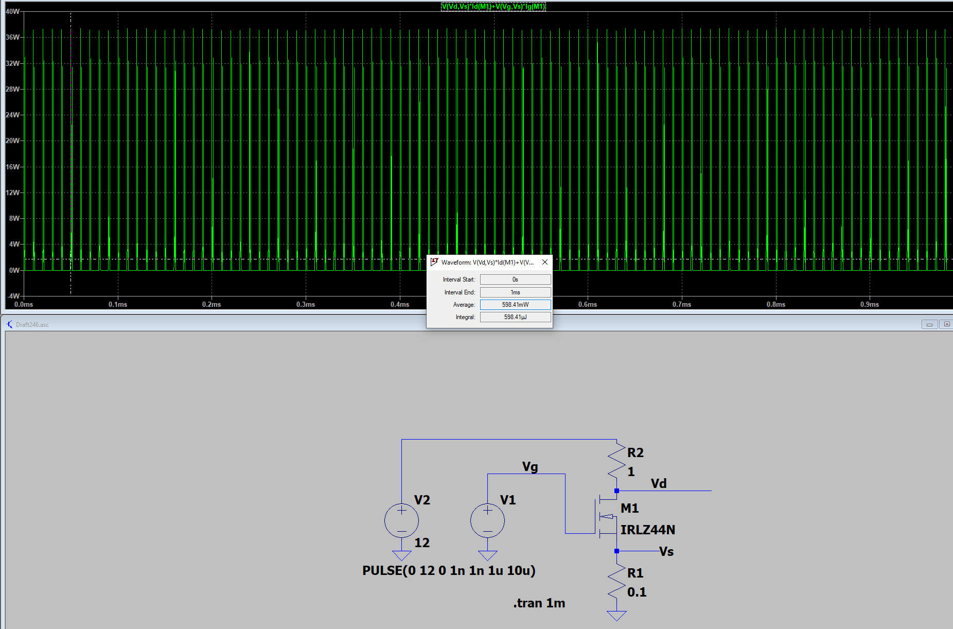
Also, using my model for the IRLZ44N I actually get about 600mW for the power dissipation.

enter image description here

\$\endgroup\$
1
  • 1
    \$\begingroup\$ There is a ground connection (several, actually) internal to the MOSFET model, which explains why LTspice didn't just outright refuse to simulate it at all. This is probably not a good sign for the quality of the model, though. \$\endgroup\$
    – Hearth
    Commented Sep 28 at 13:10
2
\$\begingroup\$

Your assumption is wrong; LTspice is correct. A negative power value indicates power being returned to the circuit from the device; a capacitor or inductor discharging stored energy.


In general, for any device, \$\sum_n \mathrm{V}(n)·\mathrm{I_x}(n)\$ (where \$\mathrm{V}(n)\$ is the voltage at pin \$n\$ relative to an arbitrary (but consistent) reference, and \$\mathrm{I_x}(n)\$ is the current into pin \$n\$) is a valid formula for calculating the instantaneous power in the device. Proving this is beyond what I'm willing to do this early in the morning, but to get an intuitive feel for it, consider these two circuits:

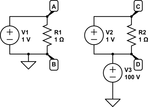
schematic

simulate this circuit – Schematic created using CircuitLab

I think you can agree that the power dissipated in R1 is equal to the power dissipated in R2, right? They are both 1 Ω resistors, and both have 1 V across them. The only difference is what point you call 0 V.

Now, let's consider the resistor on the left. The ground-referenced voltage at pin A is 1 V, and the current into pin A is \$\frac{1\ \mathrm{V}}{1\ \mathrm{Ω}}\$ = 1 A. The ground-referenced voltage at pin B is 0 V, and the current into pin B is -1 A (negative, as positive is defined as into the pin). Now, with the formula from earlier, we get $$\begin{align}\mathrm{P(R1)} &= \mathrm{V(A)}·\mathrm{I_x(A)}+\mathrm{V(B)}·\mathrm{I_x(B)}\\ &= 1\ \mathrm{V}·1\ \mathrm{A} + 0\ \mathrm{V}·-1\ \mathrm{A}\\ &= 1\ \mathrm{W} + 0\ \mathrm{W}\\ &= 1\ \mathrm{W}\end{align}.$$

This, of course, is an excessively complicated way to calculate the power in this resistor, but the general utility in the context of SPICE (which works entirely based on ground-referenced node voltages and branch currents) is clearer when you apply the same logic to the circuit on the right: $$\begin{align}\mathrm{P(R2)} &= \mathrm{V(C)}·\mathrm{I_x(C)}+\mathrm{V(D)}·\mathrm{I_x(D)}\\ &= 101\ \mathrm{V}·1\ \mathrm{A} + 100\ \mathrm{V}·-1\ \mathrm{A}\\ &= 101\ \mathrm{W} - 100\ \mathrm{W}\\ &= 1\ \mathrm{W}\end{align}.$$

Ignoring the current leaving pin D would result in overestimating the power consumption of the resistor by over 100 times!

Note that in this simple two-pin case, this is equivalent to the standard formula for power in a resistor: since \$\mathrm{I_x(A)}=-\mathrm{I_x(B)}\triangleq I\$ by charge conservation, $$\mathrm{V(A)}·\mathrm{I_x(A)}+\mathrm{V(B)}·\mathrm{I_x(B)}\\ = \mathrm{V(A)}·I+\mathrm{V(B)}·-I\\ = \mathrm{V(A)}·I-\mathrm{V(B)}·I\\ = (\mathrm{V(A)}-\mathrm{V(B)})·I,$$ which is the standard formula for power in a resistor.

\$\endgroup\$
9
  • \$\begingroup\$ Wouldn't that mean a lower overall dissipation of the circuit, but still extra dissipation in the mosfet? \$\endgroup\$
    – hennep
    Commented Sep 27 at 12:20
  • \$\begingroup\$ @hennep I'm not sure what you're asking, honestly. \$\endgroup\$
    – Hearth
    Commented Sep 27 at 13:51
  • \$\begingroup\$ What I meant was, returning power from the gate charge to the circuit lowers the power consumed by the circuit, not the mosfet. Not the complete gate charge is dissipated in the mosfet. A part of the dissipation that is lost in the gate depends on the resistance of the bond wire/internal gate circuit. I think that V(G)*Ix(U1:G) is not correct. Also in V(D)*Ix(U1:D)+V(S)*Ix(U1:S) the gate current is part of Ix(U1:S), so it is calculated twice. A better way would be Ix(U1:D)*(V(d)-V(s)) for the drain-source part. \$\endgroup\$
    – hennep
    Commented Sep 28 at 12:53
  • 2
    \$\begingroup\$ @hennep Returning power from the gate capacitance to the circuit means that the transistor's gate is sourcing power, the capacitor is discharging. This energy is not dissipated within the MOSFET, but it was counted earlier when the gate charged up. You can think of this returned energy as correcting an earlier miscount (counting stored energy in addition to dissipated energy), if you want. || Σₙ V(n)*Ix(n) is a general formula that correctly calculates the power dissipated in any device; if this is your issue, give me a moment and I'll expand on this answer. \$\endgroup\$
    – Hearth
    Commented Sep 28 at 13:04
  • \$\begingroup\$ @hennep Is that better? \$\endgroup\$
    – Hearth
    Commented Sep 28 at 16:52

Your Answer

By clicking “Post Your Answer”, you agree to our terms of service and acknowledge you have read our privacy policy.

Not the answer you're looking for? Browse other questions tagged or ask your own question.