1
\$\begingroup\$

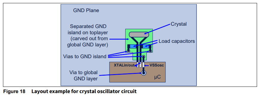
I am going through this material from Infienon.Below is the XTAL layout given in the document.

enter image description here

The explanation for this arrangement is given below.

enter image description here

What I understood from this document is they are providing a separate GND for XTAL for avoiding XTAL noise to couple to main ground(Global GND).

And also it says that at one point we need to connect this GND Island of XTAL to Global GND.Here using VSSosc.

My question is in this case also XTAL noise can couple to Global GND using that one connection(XTAL GND is connected to Global GND at one point).Then what is the advantage of this GND Island

\$\endgroup\$

1 Answer 1

1
\$\begingroup\$

The whole point of ground is to create capacitance to return high speed currents to their source.

Placing the grind around the crystal increases capacitance and lowers inductance allowing for better sinking of currents.

It also allows for less radiation which is what designers want if they want to pass EMI tests

\$\endgroup\$
1
  • \$\begingroup\$ "Placing the grind around the crystal increases capacitance and lowers inductance" may I know how this happens \$\endgroup\$
    – Confused
    Commented Nov 4 at 9:16

Your Answer

By clicking “Post Your Answer”, you agree to our terms of service and acknowledge you have read our privacy policy.

Not the answer you're looking for? Browse other questions tagged or ask your own question.