12
\$\begingroup\$

I need some help with the layout of a power supply. I botched the first two iterations as I do not have the necessary experience, and I would like to avoid another costly run.

For the sake of completeness, here is the previous (related) question: Noise problem with buck/boost switching regulator

My device is powered by a Lithium-Ion battery, but needs an operating voltage of 3.3V. Thus, Vin = 2.7-4.2V, Vout = 3.3V. I decided to use a LTC3536 buck/boost switching regulator: http://cds.linear.com/docs/en/datasheet/3536fa.pdf

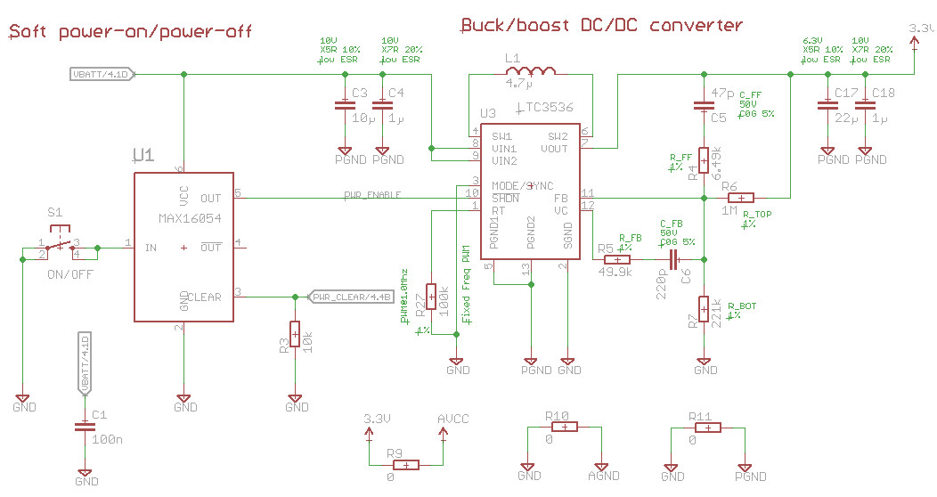
I basically used the reference implementation (page 1 of the datasheet) for a 1A/3.3V power supply. Here are the schematics:

enter image description here

There are three separate ground planes: PGND, coming from the battery and connecting to the LTC3536; GND, the signal ground which branches off from pin 3, and AGND, used for analog sensors etc which branches of from the GND plane.

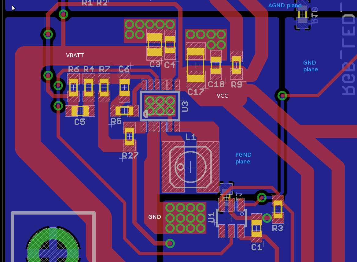
This is the latest version of the 2-layer board. Red is top, blue is bottom layer. It's quite close to LT's demo board. I annotated the different ground planes, as well as VBATT and VCC.

enter image description here

Design considerations

I tried to adhere the recommendations that I found in the datasheet and the answers I got on the previous question. I use 3 different ground planes as described above, connected in a single point using a 0 Ohm resistor. I tried to use a star-like approach for routing VCC. AVCC is connected to VCC using a 0 Ohm resistor.

Questions

  1. One of the problems with the previous design was that I connected the exposed pad of U3 using vias at the side of the chip. This required a lot of space. I now realized that LT added on their demo board the vias directly under the exposed pad. I didn't know that this is possible - do I need to do something special to these vias?
  2. I am quite unsure regarding the placement of the ground planes. At the moment, the GND plane tees off from pin 2/3, and is connected to the AGND and PGND plane using a 0 Ohm resistor. Placement of this resistor is kind of random atm.
  3. The whole circuit is switched using a MAX16054 soft power-on/off IC, which connects to SHDN of U3 (pin 10). The MAX16054 is connected to VBATT and GND (not PGND). Might this cause problems?

Any comments would be greatly appreciated!

\$\endgroup\$
6
  • 3
    \$\begingroup\$ relevant reading: analog.com/library/analogdialogue/archives/41-06/… \$\endgroup\$
    – Phil Frost
    Commented Jul 2, 2013 at 14:20
  • 1
    \$\begingroup\$ also: electronics.stackexchange.com/questions/74509/… \$\endgroup\$
    – Phil Frost
    Commented Jul 2, 2013 at 14:22
  • \$\begingroup\$ The first doc linked by @PhilFrost it's great. It helped me to understand how route the SMPS. I highly recomend it. \$\endgroup\$ Commented Jul 4, 2013 at 12:25
  • \$\begingroup\$ @arnuschky I don't agree with the separated GNDs. It sometimes create more problems that it solves. In some way the output capacitors of your SMPS are the power supply of your circuit. So let's consider C17 and C18 your power supply. Their Vcc pins powers all your circuit BUT their GND point is isolated (Ok. not isolated but too far) from your circuit! In my opinion this is a really big problem. Why do you don't consider join PGND and AGND? Attention with your feedback track. It cross a GND split! Keep it over the same power plane. \$\endgroup\$ Commented Jul 4, 2013 at 13:52
  • \$\begingroup\$ OK thanks, I will fix the power plane. I am not sure if I should join the PGND and AGND. Don't I run the risk of seeing the currents from the SMPS in the analog circuits? Regarding the output caps: According to you, I should move them to GND? This is the opposite from what AndyAka said in the other question. \$\endgroup\$
    – arnuschky
    Commented Jul 4, 2013 at 22:45

2 Answers 2

7
\$\begingroup\$

I hope I don't contradict anything said on the previous question's answer!!!

The feedback point should be taken from as close to the output pin as possible. Note the track on the non-component side of the LTC3536 document.

I'd use a full ground plane on the underneath all round but the low voltage end of R7 needs to get to pin 2 and then pin2 needs to star point under the chip to local full ground plane.

I wouldn't tee off R27 (and pin 3) to feed the top copper that connects to the bottom copper (GND Plane) - I'd let (what you've called) GND plane flood thru to power ground where R11 is and as far up as nearly the analogue ground plane.

The track from pin 10 should attempt to keep to the top layer as much as possible so as not to interrupt ground planes underneath.

\$\endgroup\$
5
  • \$\begingroup\$ Hey Andy. Thank you for your comments (again!) I started to implement the changes when I was running into some problems. I now redid the layout very close to LT's demo board. Using this layout, your first and last point is fixed. Unfortunately, I did not fully understand what you said about the ground planes. The GND plane now tees off pin2/3, and the AGND is connected to that plane separately. Same for R27. Is it correct like this? \$\endgroup\$
    – arnuschky
    Commented Jul 3, 2013 at 17:14
  • \$\begingroup\$ @arnuschky Which bit about the gnd plane didn't you follow? \$\endgroup\$
    – Andy aka
    Commented Jul 3, 2013 at 21:17
  • \$\begingroup\$ What I don't understand is this: I use a full plane for power ground under the chip (bottom layer). The pins 5 and 13 connect there, as well as the input and output caps. How can I then put another plane for signal ground (pin 2) under the chip if I have only 2 layers? What I did not is to have the signal ground (GND plane) a bit further away, lead pin 2 there and star of at this point (see block of 4x3 vias), but I am unsure about this star point. \$\endgroup\$
    – arnuschky
    Commented Jul 4, 2013 at 7:21
  • 2
    \$\begingroup\$ GND connections (as opposed to PGND) don't have a plane - they star point into PGND and must not carry any currents related to input power source and output load. PGND is the plane which is underneath the chip and underneath the PCB. Any components that connect to "GND" (like R7) connect to pin 2 which then routes directly to PGND. \$\endgroup\$
    – Andy aka
    Commented Jul 4, 2013 at 8:14
  • \$\begingroup\$ I have the impression that I misunderstood something substantial here. Currently, I have three planes, one for PGND, on which all the high-current paths of the converter should stay, one for "normal" GND, that provides ground connections to all other devices (ICs etc), and one for AGND, that provides ground for analog components (sensors etc). The GND plane is connected to PGND and AGND in one point each. \$\endgroup\$
    – arnuschky
    Commented Jul 4, 2013 at 9:11
5
\$\begingroup\$

Answering my own question regarding the vias in the exposed pad of U3:

As I feared, it's not so straight forward to put vias into a pad. Solder might flow through the via and can create a mess on the other side, and a bad connection of the component side. See these links for example:

Nor sure how I will resolve this. Quite nice of LT to make the demo board depend on this. I see tree options:

  1. have the vias plugged (expensive)
  2. move the vias away from the pad (might incur other problems as components can't be placed close enough)
  3. make via diameter smaller and hope that this is sufficient

Neither of these options are really satisfying. :(

\$\endgroup\$
2
  • 2
    \$\begingroup\$ Definitely you need plugged vias if the solder paste will deposit over them. Otherwise you'll have problems in the assembly process. There are other risky option. Make small solder mask aperture under the chip. As shows this image s3-blogs.mentor.com/tom-hausherr/files/2011/04/… .In this case you can put the vias away from the solder paste areas. (Sorry, maybe it's not the best image to show this). The second option you comment it's possible but I wouldn't try the third one. \$\endgroup\$ Commented Jul 4, 2013 at 12:44
  • 1
    \$\begingroup\$ I will go with option 2. As LT does not explicitly state that the vias have to be under the pad for thermal reasons, I assume that this is ok. Thanks for your reply Jesus. \$\endgroup\$
    – arnuschky
    Commented Jul 4, 2013 at 15:35

Your Answer

By clicking “Post Your Answer”, you agree to our terms of service and acknowledge you have read our privacy policy.

Not the answer you're looking for? Browse other questions tagged or ask your own question.