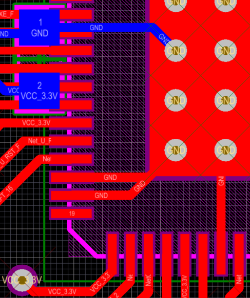
The short answer is that it depends.
If the datasheet says the center pad is meant to be connected to ground, then it is certainly not a problem to connect it to the same net as one of the pins that is also meant to be connected to ground. Electrically, at least in theory, those two parts of the chip are electrically equivalent. Connecting the center pad through a via to a ground plane and then connecting a pin through a via to that same ground plane is (again, theoretically) electrically identical to running a trace from that pin directly back to the center pad. In both cases they end up being part of the same electrical node and will have the same potential, which is what the datasheet tells you is how they should be connected.
Where that theoretical equivalence breaks down is when the electrical requirements of the circuitry reach the point where the geometry of the trace and board become a factor in their electrical performance. This could be due to high currents, where you need to consider the DC currents and hence DC resistance, but on a part like this, the concern is going to be a matter of frequency content and specifically the dynamic currents that are going to be carried by the device's power pins. Any digital device tends to consume pulses of current whenever the internal state of the device changes. In a simple digital buffer, like a 7404, there's a pulse of current each time the input and hence output change. In a microcontroller or anything else with a continuous clock and a ton of internal complexity, there's a current pulse at every clock transition as thousands or millions of internal transistors change state and the associated parasitic capacitances are charged or discharged. With a device that drives a wire, like an ethernet PHY or that USB transceiver you're working with, there will be a current pulse whenever the wire state is changed (because the whole reason we have ethernet PHYs and similar line transceivers as dedicated silicon is lines like that are hard to drive!).
Generally the faster a device is, the more significant these current pulses are to consider in designing a circuit and laying out a PCB for it. Note that 'faster' in this case is not clock frequency, or the number of times a line changes state, but how rapidly that state is changed at each transition. But devices that need to support high frequency operation inherently have to be able to change the state of their internal circuitry or an external line very rapidly, otherwise they won't be able to finish one state transition before it's time for the next one. In order to drive that state change, the device needs to be able to pull energy out of the power supply equally fast, otherwise the power supply or internal node voltages will sag and you will Have Problems. Thus, power distribution is an absolutely critical part of high speed (again, where high speed means rapid change, not necessarily frequent change!) design.
This is why a lot of datasheets and appnotes tend to spill a lot of words about the layout of power connections and decoupling, especially on high speed parts. To bring it back to the part in question, you need to carefully consider the impact that the connection strategy for a given pin will have on its operation. Any pin used to supply operating current to the part needs a sufficiently low impedance path back to the supply, or really, some reservoir of energy that can be used to drive state changes, which usually means a nearby decoupling capacitor. How nearby? Well that's the tricky part, but the primary thing you need to consider with high speed parts is the inductance between the pin and the decoupling capacitor and then the inductance from the capacitor to the regulator or bulk capacitance elsewhere on the board. This inductance will slow down the pulses of current the IC is pulling from the supply, which reduces the effectiveness of the local decoupling and can destabilize the local power supply, especially in bad cases where the inductance can cause ringing at the power pin.
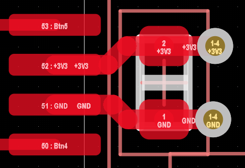
The general rule of thumb is that the track from the pad to the cap should be as short as possible and there should not be any vias between them. If there is a via or longer track back from the cap to the supply, it should NOT be between the pin and cap, but on the far side of the cap from the pin.
Here's an example of the generally preferred layout (note that this is a four layer board, and the inner power and ground planes the vias connect to are hidden):

[Side note: Ideally all tracks for chip components should come straight out of the ends of the pads, not the sides, but a symmetrical layout like this where the tracks run 'through' the pads is sort of the second best arrangement and has electrical benefits in providing minimal impedance, so it's a good tradeoff. The smaller a chip component is, the more important it is to consider how the geometry of the connecting tracks will affect the soldering process. But this is a matter of design for manufacture, not signal integrity which is the more important part of your question.]
This gives minimal impedance between the IC's power input (in this case a 200MHz Cortex M7 MCU) and the local decoupling capacitor and generally should be replicated independently on every single pair of power supply pins. Yes, that tiny little trace does matter when we're talking about the very fast pulses of current that modern digital ICs can consume.
The math behind that is the same as for any inductance calculation, the difference is that we're talking about operating frequencies in the tens or hundreds of megahertz or higher and very small inductances start to matter. The device in question here is a 5Gbps USB3 bridge, parts of it will be operating at at least 5GHz, and the transitions will inherently include even higher frequency content that needs to be considered. It's important to note that both the power and ground connections matter equally here. There are two loops formed, one from the positive power supply (wherever that is) through the board to the top of the decoupling cap, through that cap, then back through the board to the power supply, and another from the top of the decoupling cap, through the track into the IC, through the IC's internal circuitry, then back out the other track back to the cap. The latter loop needs to be kept as short as possible to keep the inductance down, because as the IC changes state and the current in that loop rapidly rises to meet the IC's demands, that change in current will manifest as a voltage over the inductance, and the voltage at the IC will drop. When that current pulse subsides, the opposite happens, and in extreme cases you can end up with nasty ringing on the power supply that can damage the IC or cause it to malfunction. Assuming the layout and hence the impedance is symmetrical between the power and ground paths of the loop, that voltage will appear on both sides of the power supply, so as the positive rail droops the ground rail rises. This happens extremely fast, and is very difficult to measure, because even a high impedance scope probe introduces parasitic electrical characteristics that will change the electrical behavior of the circuit, but it can be modeled.
The impedance between the capacitor and the regulator elsewhere on the board is less important, so vias are okay there. In fact that impedance with the capacitance forms something of a low pass filter, and in some limited cases you may enhance that with additional impedance in the form of a resistor or an inductor--but this is a bit more subtle and niche than we're really concerned with here.
In challenging layouts like dense BGA packages, vias between the part and the cap may be unavoidable, or at least may be less of an issue than the long tracks that would be otherwise required to route a power pin out to a decoupling capacitor next to the part on the top of the board, so sometimes a via down to a cap on the opposite layer is the best solution. For the same reason, some devices like PC CPUs will include capacitors directly on the IC package (which is really more like a mini PCB on its own than the more conventional leadframes used on smaller ICs).
As far as sharing vias between multiple power pins, the important thing to remember is that the impedance of a via is fixed, and using it to serve two power pins approximately doubles the electrical load on it, so doubling the current with a given impedance doubles the impact of that impedance on the circuit. Thus it's preferred to not share vias between power pins for this reason. However, in a tight layout, there are compromises, like bringing two decoupling caps back to a single location with two or more vias, which is better than a single via but not necessarily as good as two separate vias. Engineering always involves tradeoffs though, and sometimes this is an acceptable one.
So that all applies to the power pins, as far as the center pad, it generally isn't considered a power pin for the purposes of power delivery unless the device has no other power contacts. However if it's electrically connected to ground then it does contribute to maintaining a low impedance ground reference for the IC, so even if a ton of vias aren't needed for thermal reasons you generally want some for electrical impedance.
For pins that are not used to supply power to the part or to otherwise carry significant currents, layout matters far less. High speed signal lines of course need to be designed for their electrical requirements as well (mainly in terms of trace impedance and other transmission line layout concerns). Generic IO lines, or configuration pins that need to be tied high or low generally don't matter much at all. These can usually be routed to the most convenient connection point or via, and if a via is good enough for one of your power pins it won't be adversely affected by the small amount of current to hold a configuration pin low.


