1
\$\begingroup\$

Is it possible to use pins of Spartan-6 bidirectional. (switch between input/output)

The following is the situation: I have a high speed ADC and DAC, but this do not have to opperate at the same time. The ADC and DAC both have an enable line that make the input (for DAC) and output (for ADC) High Z.

Now i was thinking i could use the datalines D0 - D11 in this case for both ADC and DAC, only i do not know how i can switch a FPGA pin from input to output whitin my VHDL code. Does somebody know this or has experience with this?

example FPGA pin 1: high is enable ADC Low en enable DAC

When pin 1 = high FPGA pin 2 to 14 must be inputs, since ADC is connected

When pin 1 = low FPGA pin 2 to 14 must be outputs, since DAC is connected

I can set a pin to input or output in the plan ahead from ISE, but cannot find a bi-di option or such.

Also if this is possible how much time does it take the spartan-6 to switch from input to output and <>?

\$\endgroup\$

1 Answer 1

4
\$\begingroup\$

Nearly all I/O pins on nearly all FPGAs/CPLDs can be configured as either bidirectional, an input or an output. Without bidirectional pins, you couldn't implement bidirectional data buses for memory chips like RAMs and Flash EPROMs.

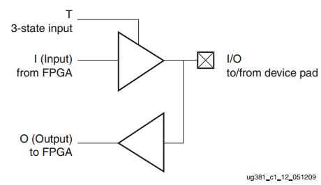
The general case for the I/O pin interface buffer circuit within an FPGA is: an output buffer that can be tri-state or driving; an input buffer.

When you configure an I/O pin as an input, the drive/tri-state control for the output buffer is tied to 'always tri-state' and just the input buffer is used.

When you configure an I/O pin as an output, the drive/tri-state control for the output buffer is tied to 'always drive', the output buffer is used and the input buffer is not used.

When you configure an I/O pin as bidirectional, it's all used.

enter image description here

Have a look at Xilinx document UG381 'Spartan-6 FPGA SelectIO Resources'. This explains all about how the I/O pins work. It includes the above diagram which shows the tri-state driver and input buffer. You'll find plenty more text on FPGA pin drivers on the internet.

To implement this in VHDL, create some internal signals called 'dataToPins', 'dataFromPins' and 'dataDriveEnable'. Then for your data bus 'DATA_BUS' you can use:

DATA_BUS <= dataToPins when (dataDriveEnable = '1') else (others => 'Z'); dataFromPins <= DATA_BUS;

The first line implies the tri-state output driver. You could use DATA_BUS as your input signal but using the second line and 'dataFromPins' as your input signal highlights to others what you're doing.

\$\endgroup\$

Your Answer

By clicking “Post Your Answer”, you agree to our terms of service and acknowledge you have read our privacy policy.

Not the answer you're looking for? Browse other questions tagged or ask your own question.