8
\$\begingroup\$

I am trying to teach myself how to make integrated circuits and I'm having trouble integrating an AND gate into the circuit though.

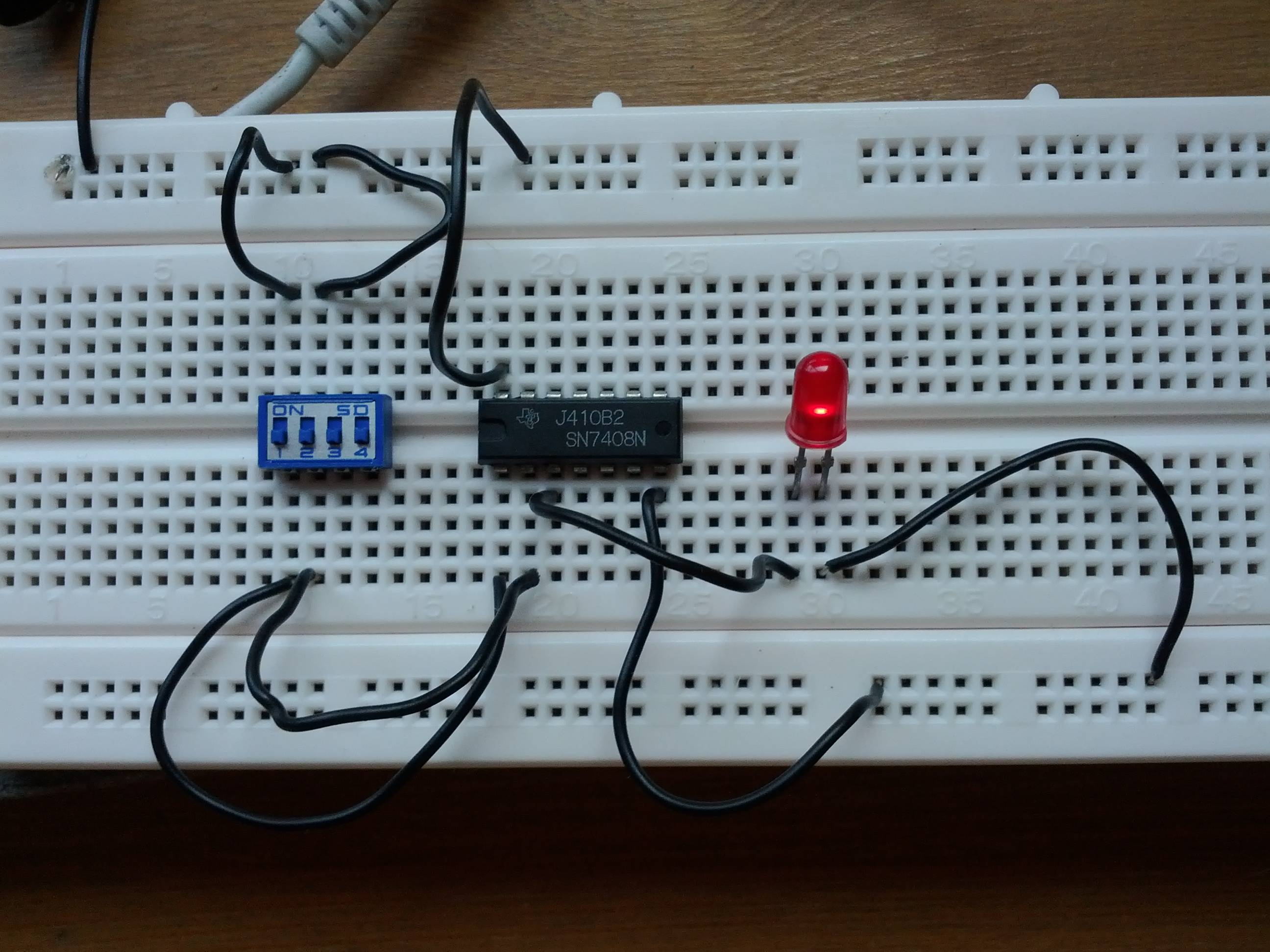
I took a picture of it. The voltage running across the power rails is 4.7 V (the chip is TTL logic, I figured it would be enough). The gate is an AND gate 2 input 1 output (7408).

My question is why, with both DIP switches turned off, is that LED shinning?? It seems that the current doesn't run through the 'AND' circuitry but through the VCC and out through the supposed to be 'output of the inputs A and B'. If the connections are wrong what's the proper way to integrate the gate into IC?

Original
Yellow- Path current is supposed to follow Yellow- Path current is supposed to follow
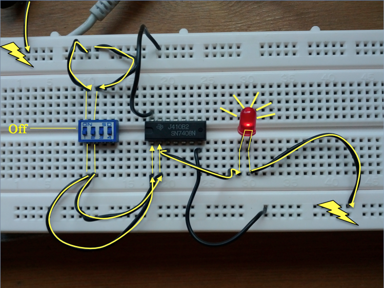
Red- Path current apparently takes -.- Red- Path current apparently takes -.-
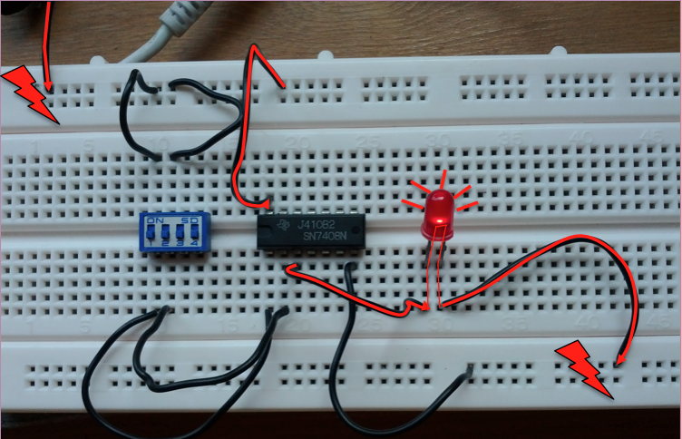
\$\endgroup\$
3
  • 7
    \$\begingroup\$ Great illustrations :) \$\endgroup\$ Commented Jun 17, 2012 at 17:20
  • \$\begingroup\$ I think you have a fundamental misunderstanding about how the circuit works. The current that flows through the LED is not also flowing through the switches. The switches only provide control signals that direct circuits inside the AND gate to either provide current to the LED or not. Therefore, we can connect the switches to ground and still get the control signals that will ultimately cause current from Vdd to be directed to the LED. \$\endgroup\$
    – Joe Hass
    Commented Feb 15, 2013 at 12:05
  • \$\begingroup\$ For your next circuit, instead of virtually coloring the wires, use really differently-colored wires. This helps a lot! \$\endgroup\$
    – Ali Alavi
    Commented Jan 21, 2014 at 21:29

2 Answers 2

13
\$\begingroup\$

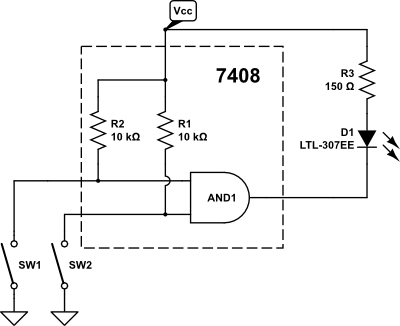
You connected the DIP switches between Vcc and the AND gate's input, and that's wrong. A floating TTL input (DIP switches off) is seen as logical 1, and when you close the switch you just enforce that 1. So inputs are always seen a 1, and output will be 1, and the LED will light.

Two things:

  1. connect the DIP switches between the inputs and ground
  2. connect the LED between output and Vcc. The logic will be inverted, but the output can sink more current than it can source, and your LED will light more visibly. Check the LED's polarity: the anode goes to Vcc. You also have to add a 150 \$\Omega\$ resistor in series with the LED to limit it's current.

The right configuration, with inverted output

\$\endgroup\$
11
  • \$\begingroup\$ hmmm... I agree with the resistor bit, but I'm having a hard time understanding what you mean by connecting the DIP switches between the AND gate's inputs and the ground? Would that be after the AND gate's output and the ground? so wouldn't that defeat the purpose of the DIP switches' ability to control whether the input would be 1 or 0 (supposedly) \$\endgroup\$ Commented Jun 18, 2012 at 4:52
  • \$\begingroup\$ You want to use the DIP switches to switch between 1 and 0. But like I explained, at the moment inputs will always be 1, also when the switches are off. So connect them between the inputs and ground, so that closing a switch will make that input low. The output has nothing to do with it. \$\endgroup\$
    – stevenvh
    Commented Jun 18, 2012 at 5:04
  • \$\begingroup\$ Thanks for writing back so quickly! OK so atm my input flows in like this: V+ --> DIP --> AND Gate Inputs. How do you get ground (V-) involved? or by ground do you mean something other than V-? \$\endgroup\$ Commented Jun 18, 2012 at 5:29
  • 1
    \$\begingroup\$ @abdullahkahraman: but look how prettier they are now, with the dots :) and without the black bar \$\endgroup\$
    – clabacchio
    Commented Jun 18, 2012 at 8:40
  • 1
    \$\begingroup\$ @valentine - the dashed rectangle in clabacchio's schematic is your 7408, so the pull-up resistors are inside the IC, you don't have to add them yourself. \$\endgroup\$
    – stevenvh
    Commented Jun 18, 2012 at 12:04
5
\$\begingroup\$

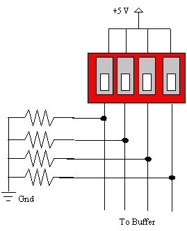
As stevenvh said, connecting the dip switch between Vcc and the And ground makes a floating state when the switch is off. I just want to add that instead of connecting the DIP switches between the AND gate's inputs and ground, you can connect them as shown using a pull down resistor, or use a pull up resistor and take inputs from the Vcc side instead. The inputs are buffer in the diagram:

enter image description here

It's just another way of doing things, but I think it feels more like a switch that way. I would have liked to add this as a comment but I don't have enough rep yet:).

\$\endgroup\$
1
  • 2
    \$\begingroup\$ With bipolar (real) TTL logic inputs, it is best to connect switches between the input pin and ground, as the inputs source current, and, if a resistor is used to pull the input low, a fairly low value resistor is required to ensure that the input is seen as a low. \$\endgroup\$ Commented May 12, 2013 at 16:55

Not the answer you're looking for? Browse other questions tagged or ask your own question.