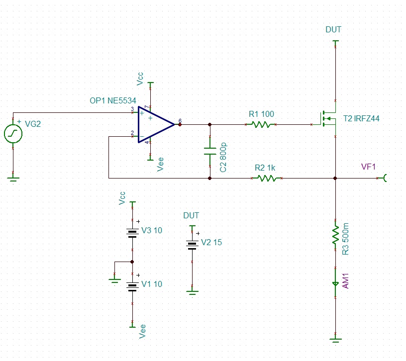
Without R1, R2 and C2, the circuit will be unstable because T1 has gate capacitance and the bare op-amp has a high output impedance (500-ish ohms sticks in my head as typical for most op-amps, but it's hard to get solid numbers). That R-C circuit is inside the feedback loop, and it causes enough phase shift to make the collection oscillate.
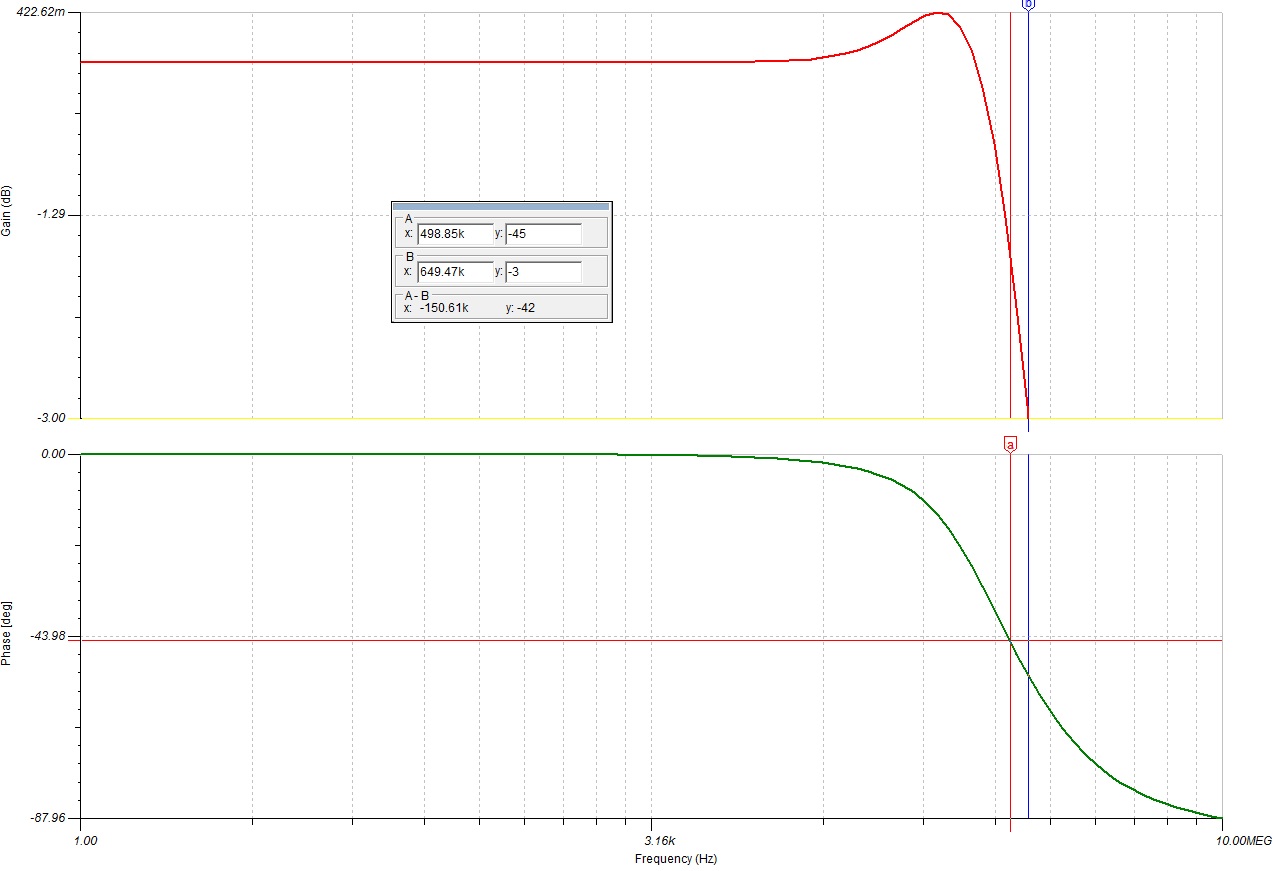
R1 isolates the op-amp output somewhat from the gate capacitance. C2 and R2 decrease the overall bandwidth of the op-amp to roughly 1/(R2*C2) radians/second. This compensates the circuit for the capacitive load.
I'm not sure of the best way to break the loop, but if you just connect a resistor to the - input of the op-amp (10k or so) and drive it with a sinusoid, you should be able to monitor the output to see if it looks well behaved. You'll basically be inferring the open-loop characteristics from the closed.
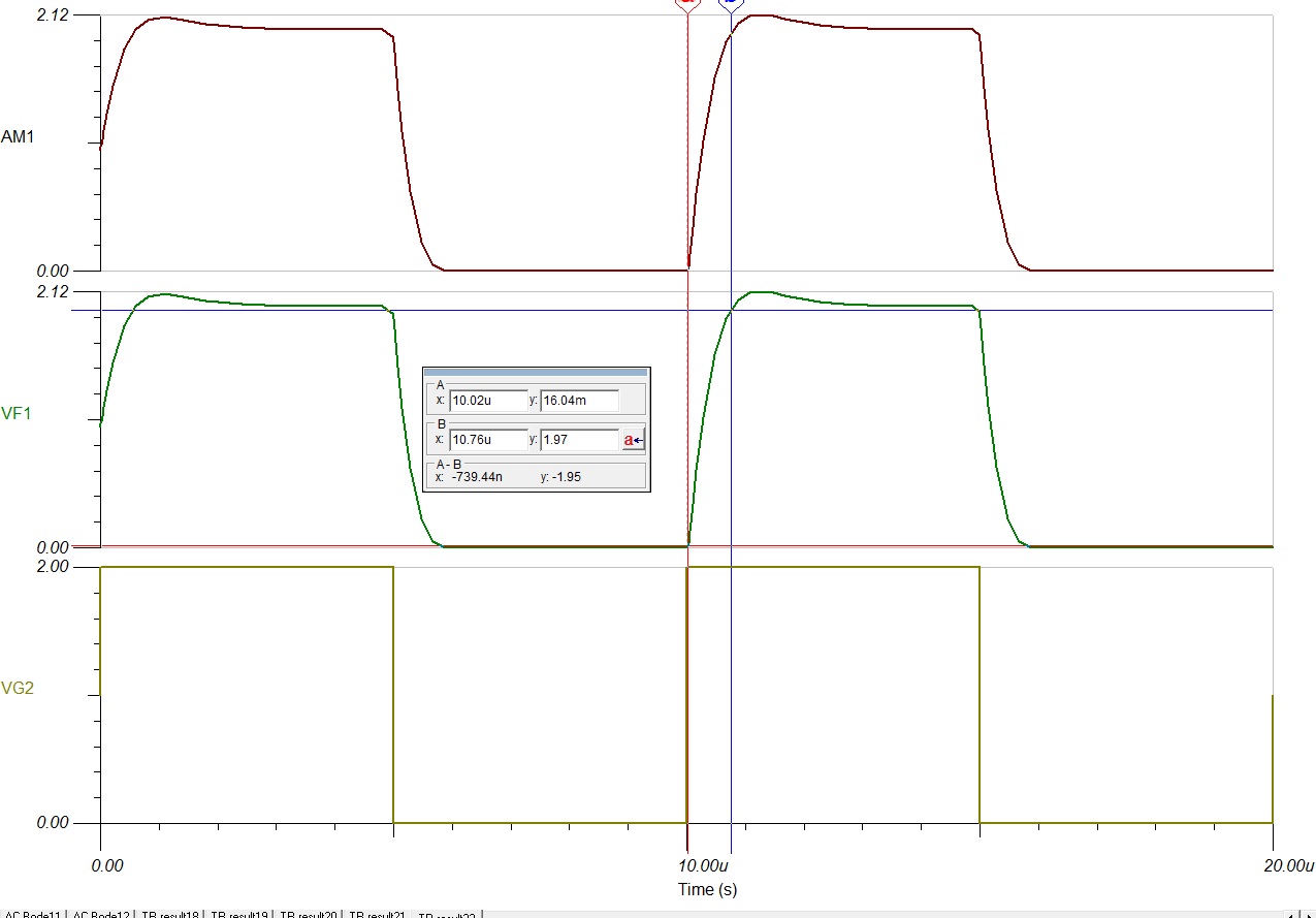
For a faster rise time, probably the best thing you can do is to find an op-amp that has a lower output impedance. That's not a data-sheet number; I'd look for devices that are designed to drive a lot of current, or are designed to drive capacitive loads.
If you want to get a bit out on a limb, choose a nice fast, small BJT (with low base capacitance!) and connect it as an emitter follower ahead of R1. You may have to add a resistor to ground to help turn the FET off (and to heat up your board's surroundings -- you didn't want your circuit to be TOO low power, right?).
Note that this isn't a place where I'd trust simulation much -- you'll want to prototype this with the specific op-amp you're going to use. If you can get the attention of an applications engineer you may want to work with them -- sometimes those guys have the sort of inside information you need.


