3
\$\begingroup\$

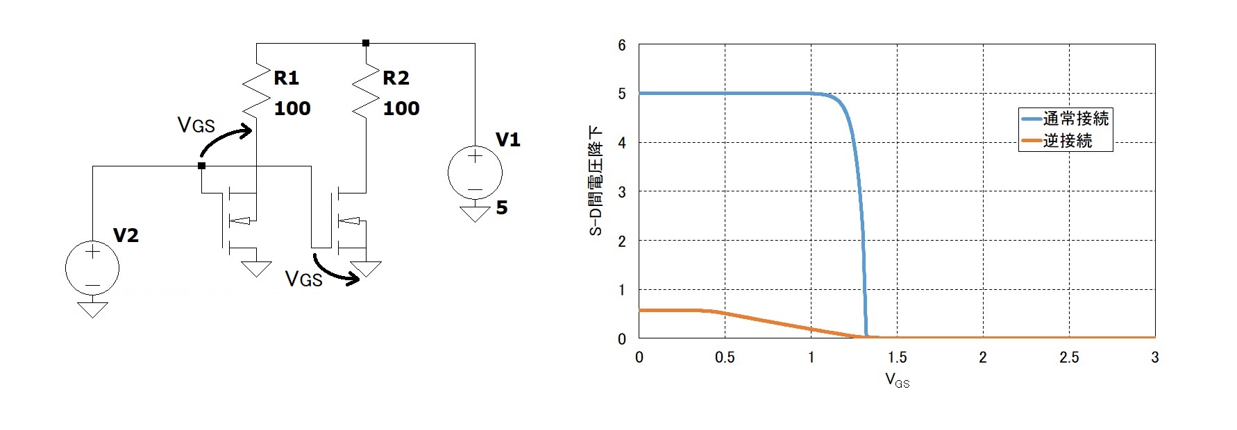
The circuit shown below is implemented using two AO3400 N-MOSFETs.
AO4300 datasheet here.

The right-hand MOSFET is connected with normal polarity (Vds is positive),
while the left-hand MOSFET is connected with reverse polarity (Vds is negative).

The graph at below right shows the relationship between Vgs and Vds simulated by LTSpice.
The blue curve is for the normally connected FET, and
the orange curve is for the reverse connected FET.

At low Vgs (<< Vgs(th)), the reverse connected MOSFET is conducting due to current in the body diode, resulting in a Vds value of about 0.6 V. As Vgs increases to above 0.4V , Vds starts towards GND level.

Why does the reverse connected MOSFET starts to turn on from about Vgs = 0.4 V when this MOSFET has about 1.1 V threshold?

enter image description here

\$\endgroup\$

5 Answers 5

6
\$\begingroup\$

Why does the reverse connected MOSFET starts to turn on from about Vgs >= 0.4 V when the published Vgs(th) value is 0.65V minimum?

  • Statements below regarding polarity are made for an N Channel device.
    The equivalent P Channel statements also apply.

The results that you are seeing are due to (well known to industry but less known in popular understanding) assymmetric behaviour of MOSFET Vgs / Ids characteristics at Vgs values both around and below Vgs(th)_forward.

Specifically, Vgs(th) may be effectively lower o even vey much lower when Vds is negative (but necessarily <= Vf(body_diode) and Ids_max may be very substantially higher for a given Vgs when Vds is negative. This is exactly the results that you are seeing.

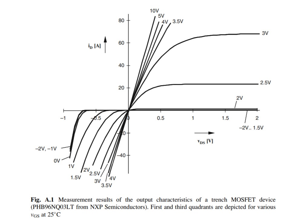
  • Examination of Fig A.1 below and the related text provides an essentially complete description show WHAT you are seeing happen.

  • For a description of WHY (for the brave :-) ) see the cited reference and related material below.

Note that while the paper indicates that the information relates to TRENCH MOS devices it also notes

    This characteristic behavior is not exclusive of trench MOS technologies 
    as it may also occur in other types of vertical MOSFETs such as DMOS, 
    CoolMOSTM, and planar structures.

Their following summation explains what you are seeing.
Note that the numerical values relate to the device they are dealing with and are similar in nature but somewhat different in absolute values to your example.

"From the measurement results it can be observed that:

  • The body diode forward characteristic seems to be modulated by voltage Vgs in the sub-threshold region, even at negative Vgs values down to 1 V [for the device in question].

  • At a given Vgs in the threshold region (i.e., voltage Vgs close to Vgs(th)), the drain current magnitude in the third quadrant is much larger than that in the first quadrant, also at low Vds. For instance, at Vgs = 2 V and Vds = -0.5 V the drain current reaches 40 A. In the first quadrant however, the maximum drain current at the same Vgs is about only a few amps.

  • A symmetric characteristic between the first and third quadrant appears ... at high Vgs.

_____________________________________________

This 15 page appendix Third Quadrant DC Output Characteristics of Low Voltage Trench MOSFETs* provides a useful introduction to the subject, and there is much other material available 'on web'.

  • *In text T. Lo´pez et al., Voltage Regulators for Next Generation Microprocessors, DOI 10.1007/978-1-4419-7560-7, # Springer ScienceþBusiness Media, LLC 2011

The following quotes (edited for brevity) are drawn from the above text:

  • In the following subsections the third quadrant output characteristics is described in more detail by looking at the internal structure of the device and analyzing the origin of this significant reverse current conduction.

  • Semiconductor manufacturers typically specify the DC output characteristics of power MOSFETs in datasheets, ... Yet, such specification only refers to the operation in the first quadrant, ... . Regarding the third quadrant, i.e., voltage Vds is negative, only the body diode forward characteristic is usually specified for zero volts Vgs. No further information about the channel current in the third quadrant and its Vgs dependence is provided.

    In circuit simulations ...

    • it is usually assumed that the first and third quadrants are symmetric
    • and that the body diode forward characteristic is independent on vGS [1, 2].
      .

    As shown in Fig. A.1, such assumption is not always valid. The plot depicts experimental results corresponding to the output characteristics of an N-channel power trench MOSFET (PHB96NQ03L)
enter image description here

______________________________

Your device behaviour for comparison.
If the device behaved symmetrically you would expect the 'yellowish' body diode limited curve to extend out until about Vgs(th)_forward at about Vgs = 0.6V
enter image description here


Related:

This reference Power MOSFET Basics by Alpha-Omega Semiconductor - who provided the coted datasheet and presumably the correct LTSpice model, covers the observed behaviour in its graphs but seems to miss the points raised above (see page 4) in its text !

The above cited paper is cited in a number of web documents

The cited appendix is taken from this book - Voltage Regulators for Next Generation Microprocessors - copyright Springer, 2011.

\$\endgroup\$
7
  • \$\begingroup\$ I think the content in first quote and edited my question is not suitable. Certainly, in the data sheet, minimum Vgs(th) is 0.65 V, but the result of simulation represents Vgs(th) is near 1.0 V. Normally connected one and reverse connected one is the same transistor MODEL. So It is obvious that the transistor used in reverse connected one in this simulation has 1.0 V threshold. \$\endgroup\$
    – ssa2
    Commented Aug 26, 2019 at 9:36
  • \$\begingroup\$ @Sano I m sorry if my edits are not acceptable. I was hoping to assist. If you wish to change anything that I alterered in your post, please do so. || Have you looked at the paper that I cited? - it precisiely answers your question. The Vgs(th)_reverse is lower than Bgs(th)_forward and it is much "softer" with substantial current flowing at eg Vgs = 0.1V. | If you read through the text at the start of the paper you will see that it describes EXACTLY what you are seeing. | "Why" is mlore complex - see the text. ... \$\endgroup\$
    – Russell McMahon
    Commented Aug 26, 2019 at 9:47
  • \$\begingroup\$ @Sano ... Note that The reverse FET curve that you posted shows Vds of about 0.2V at Vgs = 1V. This means that V across 100 Ohms is (5-0.2) = 4.8V so Ids is about 4.8V/100 Ohms = 48 mA. This is far far far above Ids at Vgs(th) - so actual Vgs(th)_reverse must be much lower than 1V.. . The paper is EXTREMELY useful and answeres your question well. \$\endgroup\$
    – Russell McMahon
    Commented Aug 26, 2019 at 9:49
  • \$\begingroup\$ So, in MOSFET we don't have the same situation as we have in BJT's when reverse biased? When now Vbc voltage will open and control the BJT? Because it looks like that now the Vgd voltage larger than Vth opens the MOSFET instead of Vgs? \$\endgroup\$
    – G36
    Commented Aug 26, 2019 at 14:15
  • \$\begingroup\$ The reverse connected MOSFET's Vgd-Vds red graph in G36's anwer ,looks representing the same drop down point and the same width between drop down point and GND reaching point compared with forward connected MOSFET's Vgs-Vds blue graph in the same figure. Is this coincidence? \$\endgroup\$
    – ssa2
    Commented Aug 26, 2019 at 16:32
3
\$\begingroup\$

A MOSFET is actually a 4-terminal device: gate, source, drain, and body. If you buy a discrete MOSFET in a 3-pin package then the body has been internally connected to the source. These devices are intended for use with the source terminal always connected to a lower/higher voltage than the drain for an NMOS/PMOS transistor. Furthermore there is inherently a PN junction from the body to the source and drain. In a 3-terminal device the source is shorted to the body so that junction doesn't matter. However, if we ever let the drain voltage become significantly lower/higher (NMOS/PMOS) than the source-body then we run the risk of forward biasing the parasitic body-to-drain diode.

So what happens at voltages too low to forward bias this diode? In that situation we have to consider what we really mean by "source" and "drain". For a 4-terminal MOSFET there may be no physical difference between the source and drain, so which ever of these is at the lower voltage (for an NMOS) will be, at that point in time, the source while the terminal at the higher voltage becomes the drain. What you have observed is that when the conventional sense of \$V_{DS}\$ is reversed then the source and drain terminals swap locations and the transistor can operate in the "reverse" direction.

This happens by design in analog multiplexers that use MOSFETs. For many years the threshold voltages of common 3-terminal MOSFETs were high enough that you usually didn't see significant conduction in the "reverse" direction before the parasitic body diode started conducting. Now that we have 3-terminal MOSFETs with low threshold voltages it is possible to see normal MOSFET conduction for low values of drain-source voltage that would normally be considered a "reverse" voltage.

\$\endgroup\$
4
  • \$\begingroup\$ In last section, why Vth and Vf is observed in one axis? Vth is value about Vgs, and Vf is value about Vds. I can't understand the sentence "before the body diode started conducting". Which voltage are you controlling in this context? \$\endgroup\$
    – ssa2
    Commented Aug 26, 2019 at 0:59
  • \$\begingroup\$ I am controlling \$V_{DS}\$. As long as \$V_{DS}\$ is below about 0.6V then the body diode will remain reverse-biased and will not contribute to \$I_{DS}\$. I don't know what you mean by "observed in one axis". \$\endgroup\$ Commented Aug 26, 2019 at 14:30
  • \$\begingroup\$ Sorry, I understood your sentence. \$\endgroup\$
    – ssa2
    Commented Aug 26, 2019 at 14:46
  • \$\begingroup\$ @ElliotAlderson See the paper I have referenced in my second answer (or even the graph from it in Fig A.1 that I copied. They show and then discuss at length a very marked assymmetry between forward and reverse Vgs / Ids or Vds characteristics. The reverse characteristics are generally significantly superior (in terms of ability to enhance the device to those in the forward direction. \$\endgroup\$
    – Russell McMahon
    Commented Aug 26, 2019 at 20:50
2
\$\begingroup\$

Added:

This turns out to be a far better and more useful question than is at first apparent. Such so that I am adding a second answer that focuses on the specifics involved.

While the answer below is essentially correct nd useful, my new answer highlights the known differences in 1st and 3rd quadrant Ids with Vgs below Vgs(th) in MOSFETS. Some of the "it may be that"s in my original answer are reflected in my new answer.

______________________________________________________________________

The "problem" is several fold. Some of these points look to be "nit-picking" (trivial and/or exaggerated) and to some extent they are - but your question, while a good one, also falls in the same category and we have to look at 'all the little things' to see possible causes. Ultimately, you are trying to extract very small precision data from a device at an extreme end of its operating range where either no expectation of precision applies and/or very small effects become significant.

  • Your results are simulated.
    What happens with a real world physical device?
    How good is the simulation?
    How do you know?

  • The datasheet tabular and graphed values are typical. Even a typical minimum is still typical unless stated otherwise. Table values for min/max usually are taken as hard limits as long as related conditions are also met. Graphs are almost always 'typical'.

  • It is common to look at the datasheet min / typ / max values for Vgsth at a given Ids and misapply them to what we are typically seeing in the circuit under observation. And the related datasheet curves (here figs 1 & 2 on page 3 of the datasheet) are essentially useless when peering at so low current low voltage regions of operation. The tendency is to TRY to apply them and to come up with "zero" when that is not the right answer.
    The graph in fig 2 suggest Ids ~~ 0.000 for Vgs <= about 1.4V - but where would you plot Ids = 100 mA on the Y axis ? :-).

    • In the datasheet on page 2 Vgs(th) is specified as 0.65 1.05 1.45 V min / typ / max.
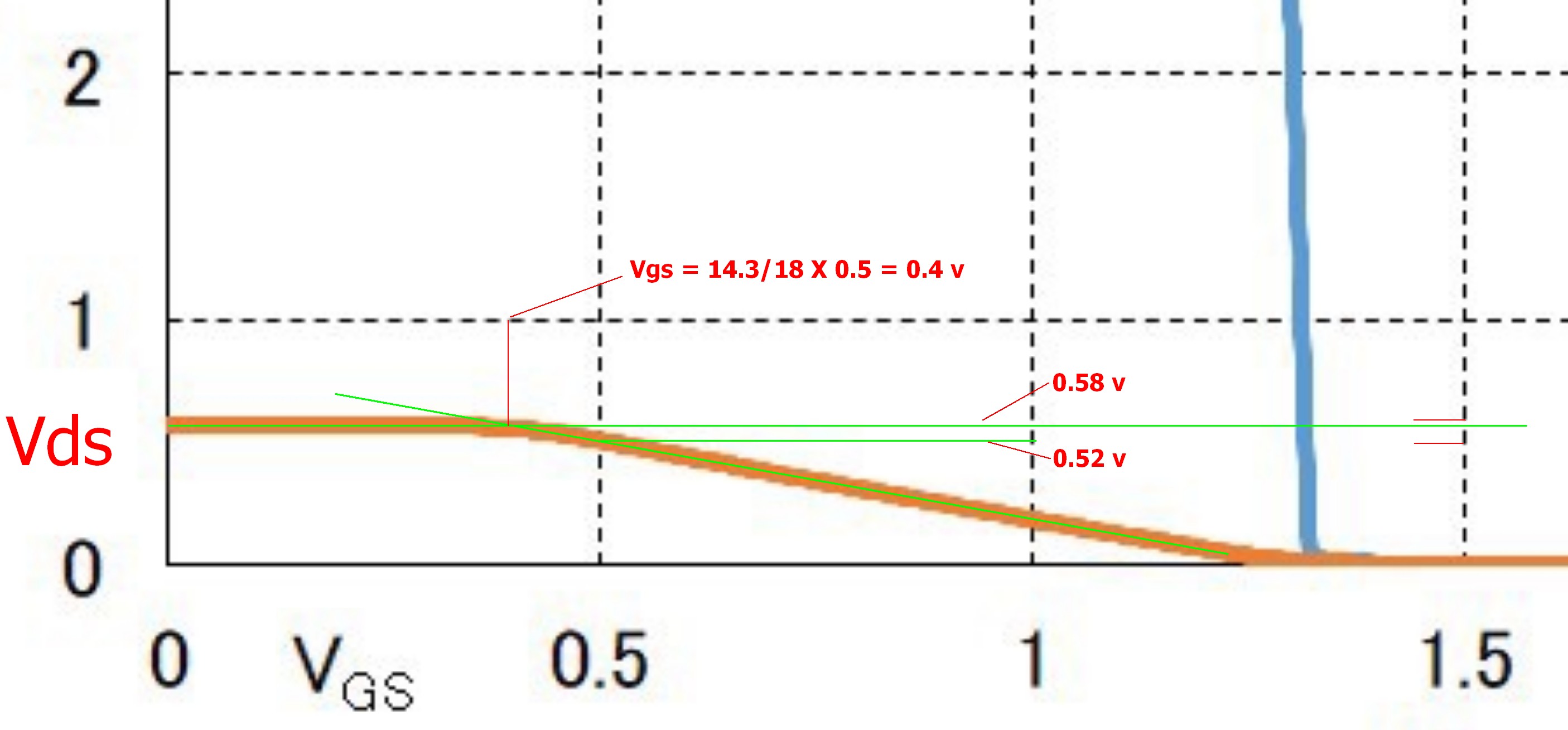
      This is NOT " ... Vgs is far from Vth ..." as noted in a comment. BUT in looking at the data sheet value an extra specification has to be noted. The given V_gs(th) is for Vds = Vgs, Id = 250 uA. Here, for the forward connected MOSFET Vds is about 20 times higher than then Vgs (5V & about 0.5V) and for the reverse connected MOSFET Vds/Vgs is high for very low Vgs (Vds ~= 0.58V due to diode for 0 < Vgs < 0.5V) and still about 50% higher (0.58V) as the MOSFET starts to conduct visibly as Vgs - 0.4V.
  • The simulation values may be optimised for typical currents which are say 0.1 - 5A and maybe 1-50A (see datasheet graphs) while here we are dealing with around 50 mA and deltas of around 500 uA.

  • The real world part may be better than the datasheet over time, as happens, this being a 2011 datasheet. So they MAY have adjusted the simulator and not the 8 year old datasheet. Which would be naughty. But happens.
    Or, the simulation values may not track the datasheet and/or real product precisely and at this level the effort required to make the model better may bot be deemed important enough.

  • The datasheet Vgs / Vds graphs are only stated as being for operation in the 1st quadrant. As you know, for a N Channel MOSFET (such as this) Vgs must always be positive for MOSFET enhancement but Vds can have either sign. But, there is no certainty that the device is absolutely symmetric electrically either for reversed Vds polarity, or for Vgs polarity with respect to Vds. If the differences were large and/or important the manufacturer would hopefully say so - but even that is not a certainty. As Vds with reversed polarity is restricted to the range of 0 to somewhere under 1V due to the body diode, the reverse Vds quadrant is usually of limited interest. But not in special cases, such as this one.

The graph below (taken from a blowup of you one) shows my interpreted / interpolated values for a number of key points. I have calculated currents at various points and relative effects of body diode and channel resistance as the channel starts to visibly conduct. I have not added them as this has already taken longer than I hoped. The above may provide enough ford for thought. If any sounds worth pursuing questions are welcome.

enter image description here

\$\endgroup\$
1
\$\begingroup\$

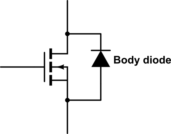
Do you know that every MOSFET has a build-in body diode between the drain and the source?

In your case, the anode of a body diode is connected to the source terminal and the cathode to the drain terminal.

schematic

simulate this circuit – Schematic created using CircuitLab

And this is why you get 0.6V when MOSFET is reverse connected. Because this diode is now in forward-bias and conducts current.

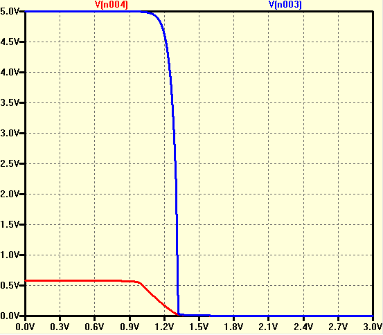
I use this one http://www.aosmd.com/products/mosfets/n-channel/AO3400

And get this results:

enter image description here

\$\endgroup\$
19
  • \$\begingroup\$ I know it, and it is written in my question. I want to know why reverse connected one is start to drop down Vds when Vgs is under Vth.(near 0.5V) \$\endgroup\$
    – ssa2
    Commented Aug 25, 2019 at 14:51
  • \$\begingroup\$ @Sano Until V2 voltage is lower than Vht the bod diode is ON and conduct current. Right? But at the time when V2 > Vth MOSFET normal (channel) current begins to flow. And MOSFET shorts out the diode current. \$\endgroup\$
    – G36
    Commented Aug 25, 2019 at 15:00
  • \$\begingroup\$ But Vds is start to drop down at 0.5V even though Vgs is far from Vth. \$\endgroup\$
    – ssa2
    Commented Aug 25, 2019 at 15:03
  • \$\begingroup\$ Do you have a MODEL for AO3400? \$\endgroup\$
    – G36
    Commented Aug 25, 2019 at 15:12
  • \$\begingroup\$ Yes. I got it from website \$\endgroup\$
    – ssa2
    Commented Aug 25, 2019 at 15:13
1
\$\begingroup\$

Sorry although this is a question from three years ago, I just came across it recently and found a more reasonable answer.

You may have noticed that for the MOSFET on the left,

  • the source voltage is positive
  • the drain voltage is ground
  • the body terminal is connected to source

Note that this refers to physical or nominal source and drain. In fact, due to the structure of the MOSFET, the source and drain are the same, so the current can flow from both directions.

From a circuit perspective, the "source" of an Nchannel MOSFET is the terminal at the LOWER voltage and the "drain" of an Nchannel MOSFET is the terminal at the HIGHER voltage.

So you can consider the left MOSFET as the following case.

  • the drain voltage is positive
  • the source voltage is ground
  • the body terminal is connected to the drain

In this case, because the source and body voltages are inconsistent, this causes the body effect.

According to the formula of body effect, VSB is negative, so that Vth becomes smaller.

In addition, this connection will also make the body diode exist, which will make the current slightly larger.

\$\endgroup\$

Your Answer

By clicking “Post Your Answer”, you agree to our terms of service and acknowledge you have read our privacy policy.

Not the answer you're looking for? Browse other questions tagged or ask your own question.