3
\$\begingroup\$

I am trying to understand I2C data bus from this document. It explains the START-SLAVEADRESS-R/W-ACK-DATA.. as the master-slave take turns to get hold of the shared bus for mutual communication.

One thing that I could not understand is related to the sampling of the data at the SDA line. Is it done at the falling or rising edge of the SCL line or is it done at the SCL HIGH or LOW level?

\$\endgroup\$
2
  • \$\begingroup\$ For I2C is this data sampling edges requirements is part of the I2C protocol or not? Is it done on both edges? \$\endgroup\$
    – alt-rose
    Commented Nov 18, 2019 at 8:00
  • 1
    \$\begingroup\$ There are a number of different modes for I2C communication. Some list sampling at the falling edge, while some say the rising edge is an option. Best to refer to the wiki page for all the different I2C modes and specifications related to clock edges, see: en.wikipedia.org/wiki/I%C2%B2C \$\endgroup\$
    – Nedd
    Commented Nov 18, 2019 at 8:11

3 Answers 3

5
\$\begingroup\$

Data transfer-

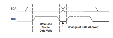
The state of SDA(high or low) can change only when SCL is low. This means SDA must be stable when SCL high.

Sampling is done while the SCL going 0 to 1 state. Changing SDA when SCL is low provides some timing margin for accurate sampling.
enter image description here

As for I2C itself is a mutual interface standard. Both sides(TX and RX) can control the SDA line in different times. So SDA pins on both sides must be birectional.

Start and Stop Conditions-

Start: when SCL:HIGH , Falling edge of SDA occurs

Stop: when SCL: HIGH , Rising edge of SDA occurs

\$\endgroup\$
2
  • \$\begingroup\$ Your last sentence contradicts the first sentence. \$\endgroup\$ Commented Nov 18, 2019 at 12:41
  • 2
    \$\begingroup\$ I think everyone understands(including you) that the last sentence means start and stop commands and the first sentence means data bits. Something strange even though you said the same thing. \$\endgroup\$ Commented Nov 18, 2019 at 14:04
4
\$\begingroup\$

The I2C interface is a de facto standard that is now controlled by NXP. Search for the NXP "I2C-bus specification and user manual", UM10204.

The standard specifies a data bit setup time before the rising edge of the clock and a data hold time after the falling edge of the clock, so a receiver could potentially use either edge of the clock, or could use a level-sensitive latch when the clock is high.

Of course, the receiver must also be able to detect the start and stop conditions where the SDA line changes while the SCL line is high.

\$\endgroup\$
3
\$\begingroup\$

From my answer from a similar question...

To be a bit more precise, the data isn't just sampled at the rising edge, but must change before the rising edge and be stable for the entire HIGH period of the SCL.
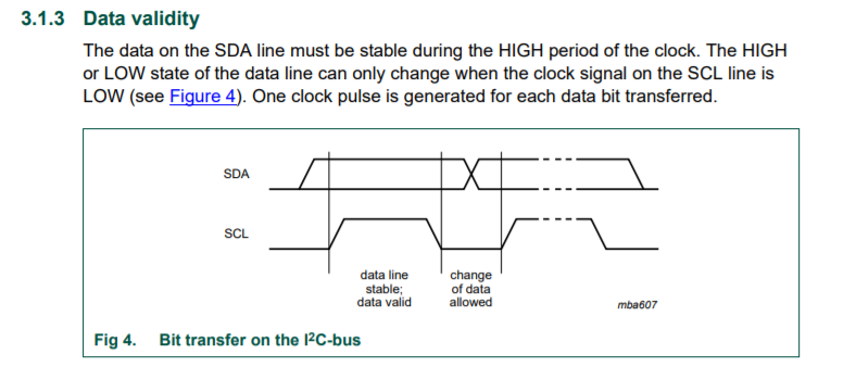
Data Validity

This screenshot was taken directly from the I2C Specification.

Note: The ACK bit must follow this as well:

enter image description here

More about timing

After reading your comments on your question you seem to be curious about whether there should be a delay after you change your SDA before you change your SCL. The answer is yes, but it's all dependent on what mode your device will operate in. See tables 9 and 10 of the specification. Table 10 specifically refers to the timings, which may be what you're interested in.

For some very basic numbers, here are the min and max for Standard-mode for data setup and hold (min in left, max in right):

Standard-mode Setup and Hold

If you notice, the data hold time has 0, but there is a caveat:

Caveat 3 for setup and hold times

This is simply restating what you see on the last row of the above picture, the maximum fall time of the SCL or SDA lines in Standard-mode must be under 300 ns, therefore the data hold time should be at least 300 ns to account for the slowest possible SCL transition.

In Standard-mode, VIHmin (the minimum input voltage to be considered high) is 0.7V. VILmax (the maximum input voltage to be considered low) is 0.3V. That means the range between 0.3V and 0.7V is unstable.

What all this means

Assuming you are operating in Standard-mode:

  • SDA must be setup (moved to a stable range) 250ns before SCL goes high.
  • SDA must be stable for the entire HIGH period of SCL.
  • SDA must be held for 300ns while SCL goes low.

Saying "while" here seems a bit strange, but it's to emphasize the 0 + 300ns minimum needed for SCL transition back to low. Typically I believe the hold time will be (1/2*SCLperiod) + 300ns. More information can be found in Table 10 of the specification to understand what operating mode you are dealing with.

\$\endgroup\$
2
  • 3
    \$\begingroup\$ While this link may answer the question, it is better to include the essential parts of the answer here and provide the link for reference. Link-only answers can become invalid if the linked page changes. - From Review \$\endgroup\$
    – Voltage Spike
    Commented May 29, 2020 at 2:20
  • \$\begingroup\$ Sure thing, let me update my answer. \$\endgroup\$ Commented Jun 1, 2020 at 22:42

Your Answer

By clicking “Post Your Answer”, you agree to our terms of service and acknowledge you have read our privacy policy.

Not the answer you're looking for? Browse other questions tagged or ask your own question.