0
\$\begingroup\$

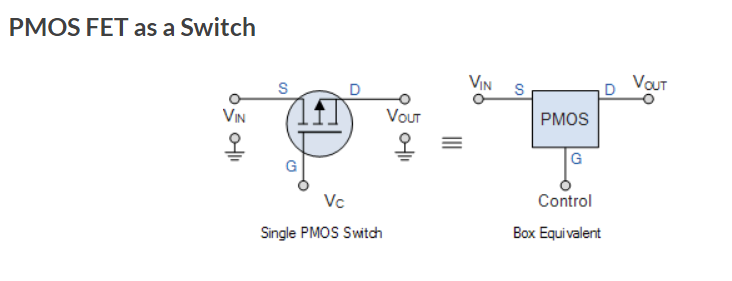
enter image description here

If I understand correctly, for a PMOS, \$V_{t} < 0 \$ and so if \$V_G < V_t\$, a nonnegligible current will flow from source to drain, whereas, if \$V_G > V_t\$, \$\text{ }i_D\$ is in the cutoff region.

However, in the context of digital circuits it's said if the gate voltage, call it \$V_C\$, is zero and hence is more negative, with respect to either the input terminal (source) or the output terminal (drain), the transistor is “ON” and in its saturation region, acting as a closed switch.

Why, in this context, does a PMOS act like a closed switch when \$V_G\$ is zero, rather than only if it's less than \$V_t\$?

\$\endgroup\$
1
  • 2
    \$\begingroup\$ The image shown has the source and drain labels swapped. \$\endgroup\$
    – Hearth
    Commented Mar 30, 2020 at 17:12

3 Answers 3

2
\$\begingroup\$

You are confused because the Vg voltage COMPARED TO "ground" (or the bottom, negative power supply rail) is zero, but compared to the source pin, it is actually negative few volts (Vgs = -x volts), and a P-channel MOSFET conducts or is turned on when the gate pin is a negative few volts (usually around -3V to -10V).
The text mentions the gate "voltage" (the correct term here would be "potential"), but it refers to it as relative to the ground (or the negative power supply rail) instead of to the MOSFETs source electrode, and that's where all the confusion is coming from.
It's really not your fault, but the fault of the person explaining it. It is possible that the author of that schematic and the related text/explanation doesn't understand it well him/herself.

Your schematic symbol for PMOS is flipped around - the arrow is supposed to be connecting on the Source side (to the left).
It would help you to use an NMOS transistor as an example to understand the switching action.
As you probably know, when the gate pin of an NMOS (N-channel MOSFET) transistor is positive compared to the source pin (also known as Vgs or gate-to-source voltage), the transistor will start conducting (a current will start flowing from drain pin to source pin).
Normally you need a few volts for Vgs to turn a MOSFET on, most often around 10V and 5V for logic-level MOSFETs, even less for special types, but usually never more than 20V as that would damage most MOSFET gates.
If you drop the voltage between gate and source to zero (Vgs=0V), the transistor will not conduct, it will be off.
Now all you need to do is flip the polarities around, and you will understand how a P-channel MOSFET works.
Don't worry if it takes you a few times to digest and understand, it is not always easy to wrap our heads around some things, even if they seem simple once we understand them.

\$\endgroup\$
4
  • \$\begingroup\$ Only in the reverse polarity diode case is it arranged with source on the right. OP has it drawn as a load switch with source on right. Unclear which the OP is asking about. \$\endgroup\$
    – DKNguyen
    Commented Mar 30, 2020 at 14:09
  • \$\begingroup\$ @DKNguyen: Both the letter S symbol on the schematic AND the text quoted in the question indicate that this is a P-channel MOSFET and that the pin source is on the left. Also, if you know about the functioning of P-channel MOSFETs and their use as switches on the positive side, you would see that the MOSFET symbol is horizontally reversed. \$\endgroup\$ Commented Mar 30, 2020 at 16:54
  • \$\begingroup\$ Oh, I see what you are getting at. The terminal labels are mislabelled relative to the symbol itself. \$\endgroup\$
    – DKNguyen
    Commented Mar 30, 2020 at 17:08
  • \$\begingroup\$ @DKNguyen: Yes. Actually, the labels are on the correct sides in regards to the circuit, but the symbol is flipped horizontally, so the labels are on the wrong sides of the MOSFET. \$\endgroup\$ Commented Mar 30, 2020 at 17:11
1
\$\begingroup\$

The gate voltage is relative to the source. So when the Vgs is less than* the threshold voltage, significant current can flow from source to drain (often threshold is specified as something like 250uA).

In your example where Vg is zero, Vgs is -Vin. So if, say, Vin is +5V then Vgs is -5V and the Rds (assuming a logic-level MOSFET) can be very low.

* greater in magnitude, but negative in sign

Example datasheet:

enter image description here

So if Vin is +5V then Rgs(on) will be less than 60m\$\Omega\$ when Vg = 0.

When off (Vg = +5V) the leakage is guaranteed to be less than -1uA at 25°C.

\$\endgroup\$
0
\$\begingroup\$

There's an error in your schematic, where the D and S labels do not correspond with the MOSFET's drain and source. For this application, the labels are correct, and the MOSFET must be flipped horizontally to be correct. I'll redraw it here, corrected. I'll illustrate the two conditions, \$V_C\$ low (ON) and \$V_C\$ high (OFF):

schematic

simulate this circuit – Schematic created using CircuitLab

Here I will call the voltage of Q1's source \$V_S\$, which is always equal to \$V_{IN}\$. At Q1's gate the voltage is \$V_G\$, which is equal to whatever control voltage \$V_C\$ you apply there.

The on/off state of the MOSFET is determined by the the difference between the voltage at the gate, and the voltage at the source. This quantity is called \$V_{GS}\$, where \$V_{GS} = V_G - V_S\$.

For P-channel MOSFETs \$V_{GS}\$ must be very negative for the MOSFET to be switched on (saturated), or close to zero to be switched off.

As you can see, on the left, when the gate is connected to a voltage much lower than the source, the difference is:

$$\begin{aligned} V_{GS} &= V_G - V_S \newline &= 0V-(+12V) \newline &= -12V \end{aligned}$$

This is very negative, and easily enough to switch Q1 on, which becomes very conductive. Effectively Q1 connects \$V_{IN}\$ to \$V_{OUT}\$.

On the right, though, the gate is held at a voltage close or equal to \$V_{IN}\$, resulting in:

$$\begin{aligned} V_{GS} &= V_G - V_S \newline &= +12V-(+12V) \newline &= 0V \end{aligned}$$

This is insufficient to switch Q1 on, and the resulting high impedance between Q1's source and drain means that \$V_{OUT}\$ is effectively disconnected from \$V_{IN}\$.

\$\endgroup\$

Your Answer

By clicking “Post Your Answer”, you agree to our terms of service and acknowledge you have read our privacy policy.

Not the answer you're looking for? Browse other questions tagged or ask your own question.