0
\$\begingroup\$

I'm making a binary input button pair with one or "1" and the other for "0" and load this input into a shift register so I need to have from these 2 buttons a persistent line for data either "1" or "0" as well as a clock signal to load the register. The clk pulse is simple since all I need is to debounce both the switches and wire them both directly to the clk pin, the pulse will be generated when the button are pressed (or released)

I'm at a loss as to how to have either a persistent "0" or "1" so when the pulse from the clk comes data can be loaded into the register.

I understand that you need a mux and/or a flip flop to achieve this but I can't figure out the wiring for the life of me.

Thank you.

\$\endgroup\$
2
  • \$\begingroup\$ Well, it could be done with some oneshots and passives. But here's a behavioral description. You could actually get parts with those behaviors and plug them in. It would be just slightly more complex (another one-shot) if you want the clock to fire just a little later. \$\endgroup\$
    – jonk
    Commented Apr 5, 2021 at 3:46
  • \$\begingroup\$ I am handicapping myself my doing this as an intro to circuit exercise, I should be able to accomplish this with nothing other than passive components and 74157(MUX), 74173(D-flip-flop)7414(Schmitt trigger), 7473(JK-flip-flop) :) \$\endgroup\$
    – Neil Ng
    Commented Apr 5, 2021 at 3:47

1 Answer 1

1
\$\begingroup\$

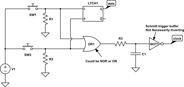
The following circuit might suit your purposes.

schematic

simulate this circuit – Schematic created using CircuitLab

R1 and R2 serve to pull down the inputs of latch1 when the temporary switches are open.

When one of the switches is closed, the first contact will cause latch one to latch that state. Further contact bounces will not alter the state of latch1.

If either of the buttons are pushed, the OR gate will give a positive output. This output will be both delayed and debounced by the RC circuit at it's output. The delayed and debounced signal is then buffered through an inverter.

Obviously, the logic can be modified in various ways while keeping the overall behavior the same. For example, the logic may be inverted, with the momentary switches bringing lines low rather than high.

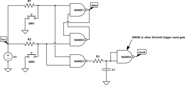
To reduce IC count, a quad NAND gate IC with Schmitt trigger inputs (such as the 4093B) could be used. Here is an example.

schematic

simulate this circuit

\$\endgroup\$
3
  • \$\begingroup\$ Thank you, I was killing myself trying to do this with a D flip-flop \$\endgroup\$
    – Neil Ng
    Commented Apr 5, 2021 at 3:53
  • \$\begingroup\$ How would you wire this with a JK flip flop instead of a latch? \$\endgroup\$
    – Neil Ng
    Commented Apr 5, 2021 at 3:54
  • \$\begingroup\$ if the JK flip flop has an asynchronous set and reset, I would use those. Essentially making a SR latch. :-) Otherwise, I wouldn't use a JK flip-flop, because it requires a clock, and the whole idea is to latch the input before the clock pulse is generated. There may be a way to do it. I'm sure there is, but it would be more complex, as far as I can tell. \$\endgroup\$ Commented Apr 5, 2021 at 3:58

Your Answer

By clicking “Post Your Answer”, you agree to our terms of service and acknowledge you have read our privacy policy.

Not the answer you're looking for? Browse other questions tagged or ask your own question.