9
\$\begingroup\$

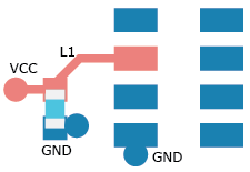
I'm a beginner in PCB layout, and have a question about decoupling capacitor routing in through-hole designs. I know that in SMT design, best practice is to place the capacitors as close as possible to the supply pin and route power from its source (supply trace or plane) first through the capacitor and then to the pin, kind of like this:

enter image description here

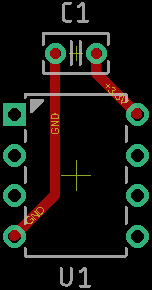
In a through-hole design, we might start like this, before pouring the power and ground planes (example in EAGLE):

enter image description here

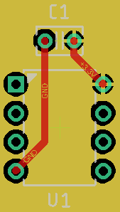
Now, when we pour the power plane, we get this by default:

enter image description here

Note that since both the capacitor pin and the IC's supply pin are on the +3.3V net, the design tool (EAGLE) has connected both pins to the plane. My questions are:

  • Does this really matter? I believe standard best practice is to force the connection to the supply to go through the capacitor before it reaches the pin.

  • If it really does matter - and I think it does - is there a way in typical PCB software (EAGLE in my case) to prevent it from connecting the IC's supply pin to the plane, so that the plane only connects to the capacitor pin, and thence via the trace to the IC pin? I know I could manually draw a keepout polygon to block the polygon pour in the area around the pin, but this would be a very tedious process to do by hand for every pin. My thinking is that if this is really electrically important, most PCB software should offer a way to deal with this.

  • Do the answers to #1 and #2 also apply to the GND pins? In this example, would it be best to (a) connect both capacitor's and IC's GND pins to the plane and not bother with a trace, or (b) trace from the IC's to capacitor's GND pin, and connect the capacitor GND pin to the GND plane?

\$\endgroup\$
11
  • \$\begingroup\$ I think the scenario between the SMD and through hole design is different - the SMD design obviously has no VCC or GND plane on top as it might be a 4 layer design but the problem would be identical on 2 layer boards. On a 2/4 layer board, won't it be better to have direct connection to power plane because it is possible via component legs and having a cap nearby also directly on the power planes, than to forcibly have long thin wires with stray inductance first going to capacitor which is then directly connected to power planes? On a SMD design it will be different as you have to have vias. \$\endgroup\$
    – Justme
    Commented Oct 15, 2021 at 9:21
  • 2
    \$\begingroup\$ How come you have routed GND as opposed to bottom (or inner layer) being dedicated to GND? \$\endgroup\$
    – winny
    Commented Oct 15, 2021 at 9:23
  • \$\begingroup\$ @winny That's part of the question, see the last bullet point. Also these pictures are only for illustration (I drew them solely to illustrate the question, it's not a real design.) \$\endgroup\$
    – TypeIA
    Commented Oct 15, 2021 at 9:25
  • \$\begingroup\$ @Justme "Won't it be better to..." I don't know, I hope an expert can tell me :) This question is about 4+ layer boards or at least boards where there are dedicated power planes. On a 2 layer board where power is typically routed on traces, this question would not apply, as you say. \$\endgroup\$
    – TypeIA
    Commented Oct 15, 2021 at 9:28
  • 1
    \$\begingroup\$ Let us continue this discussion in chat. \$\endgroup\$
    – winny
    Commented Oct 15, 2021 at 12:52

3 Answers 3

19
\$\begingroup\$

The truth of the matter is that it doesn't really matter if the current "hits" the capacitor before the pin of the IC or not. This has long been debated and recent studies have suggested that simply having the capacitor placed close to the IC is sufficient. Dave Jones of the EEVBlog did a video to help illustrate this, but he is most certainly not the only one. I believe Rick Hartley, one of the world's leading experts in high-speed board design, has also proven that it does not really matter the order in which the current "hits" the pins. In most cases, it is actually preferred to have the capacitor connected to the IC pin through a plane, as that is lower inductance than a discrete trace.

Here is Dave Jones' video: https://www.youtube.com/watch?v=1xicZF9glH0

\$\endgroup\$
6
  • 2
    \$\begingroup\$ That's a really insightful video, thanks. I've seen some of Dave Jones' other videos and love his channel. By this reasoning (and from the demonstration), I think I should just plant the decaps as close as possible to the relevant IC pins and allow both pins to thermal into the planes - the current will sort itself out. No explicit traces (since we have uninterrupted/solid power and ground planes - at least as uninterrupted as possible given a through-hole design! uninterrupted by signal traces at least!). Is that your take also? \$\endgroup\$
    – TypeIA
    Commented Oct 15, 2021 at 14:39
  • 3
    \$\begingroup\$ @TypeIA I agree, no need for discrete traces. On another note, I have never heard them referred to as "decaps". They are decoupling capacitors. Is "decaps" an actual term? More a question for the rest of the community, really. \$\endgroup\$
    – DerStrom8
    Commented Oct 15, 2021 at 16:30
  • 2
    \$\begingroup\$ Thanks again. "Decap" is just slang as far as I know, but it pops up in many circles and even in academic papers. Übrigens, mir gefällt dein Name :) \$\endgroup\$
    – TypeIA
    Commented Oct 15, 2021 at 16:47
  • 7
    \$\begingroup\$ @DerStrom8 "decap" means remove the encapsulation or package of an IC to examine the die directly. I have never heard it used for decoupling capacitors. \$\endgroup\$
    – user57037
    Commented Oct 15, 2021 at 17:14
  • 2
    \$\begingroup\$ @mkeith citeseerx.ist.psu.edu/viewdoc/… "Decoupling capacitors (decap) are often used to filter out noise in the power distribution system (PDS)." \$\endgroup\$ Commented Oct 20, 2021 at 22:09
5
\$\begingroup\$

The only thing that matters is that you keep the inductance of your track arrangement low. Inductance depends on the area between the tracks of one closed loop circuit (and regardless what else is placed inside).

So you keep it low by routing pairs this way ][ and not this way [ ].

\$\endgroup\$
6
  • 1
    \$\begingroup\$ This makes sense, and so it would come down to selecting the option that results in the smallest loop area. Current follows the path of least (complex) impedance, so does connecting via a plane present lowest impedance along the straight-line (small loop area) path between the two pins, or do we have to force it to follow the straight-line / low-loop-area path via a trace? From DerStrom8's answer I guess it's actually the former. \$\endgroup\$
    – TypeIA
    Commented Oct 15, 2021 at 14:04
  • 2
    \$\begingroup\$ For the materials and dimensions and frequencies (<GHz) involved, it makes no difference. You may want to revisit that for antenna feed tracks, or when iron parts are involved. (As a rule, don't have the most delicate loops around screw holes. But then again, don't have them separated at all.) \$\endgroup\$
    – Janka
    Commented Oct 15, 2021 at 15:08
  • 1
    \$\begingroup\$ @TypeIA - "Current follows the path of least (complex) impedance, so does connecting via a plane present lowest impedance along the straight-line (small loop area) path between the two pins, " Generally, yes. The drawback with this approach is that, if you're being careful/paranoid, you wind up with a fairly low component density since you're keeping other components away from the likely return path. \$\endgroup\$ Commented Oct 16, 2021 at 13:28
  • 1
    \$\begingroup\$ @WhatRoughBeast Yes, that's been on my mind too, but I think it's manageable. Another contributor asked me "why TH in 2021" and the answer is that I'm only doing prototypes at the moment where there is value in TH simplicity for some (not all) parts. And low density for a prototype is also ok. In a production design I'd just go SMT and pack 'em in. Thanks for the insight! \$\endgroup\$
    – TypeIA
    Commented Oct 16, 2021 at 13:54
  • 1
    \$\begingroup\$ @TypeIA - Depending on your paranoia level, you should keep in mind that the return path on a ground plane is not a infinitely thin path. Rather, you get peak current level along the shortest path, with decreasing current as you get away from that path - but in principle you get some contribution arbitrarily far away from the main path. Think of the plane as a bunch of more-or-less parallel wires arrayed out from the shortest path. The longer paths have greater resistance and less current - but they do connect the two points. \$\endgroup\$ Commented Oct 16, 2021 at 14:03
5
\$\begingroup\$

A long while back I read "PCB EMC Design Techniques" by Mark Montrose, and I think it's still a good read.

At the heart the current loop impedance is important, and that includes the inductance induced by the traces that are created specifically to guarantee that the capacitor's charge is mainly used for the IC it is decoupling. Those traces can actually decrease performance. Mark Montrose writes "Maximizing the physical width of the connection from the capacitor to planes minimizes total loop inductance". Vias add inductance as well.

So in the general case, for high frequency decoupling purposes, I'ld prefer a plane connection rather than dedicated traces. The current will "find" the shortest loop anyway.

However, there is one case where I added a dedicated trace for decoupling, and it was actually a "low frequency" issue.

I had a circuit using an SDCard used to store the results of several measurements. As far as I remember, tthe SDCard was disturbing the circuit when it was switched on caused disturbances on the measurements where we were looking for very small changes in the values.

So I ended up adding a bead, and a nettie to be able to route separate VCC and GND traces up to the SDCard directly from the LDO's output. Powering the SDCard
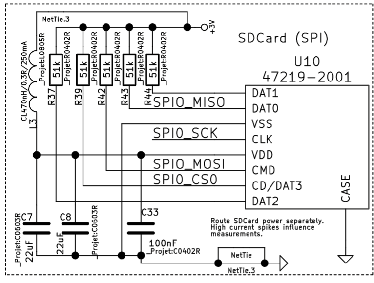
You can see the adjacent traces on the PCB, the GND trace running up to C33 and the VCC trace up to L3.
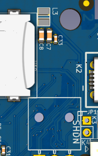
Separate power traces

The LDO is on the other side of the board in between the two holes on the left of "SHDN" in the white square. It's from that area that the traces lead up to the SDCard.

IHMO this was a low frequency "bulk" capacitor issue rather than a HF decoupling issue.

Moating

This technique essentially consists in creating areas with a local ground plane. This is something that our design group used to do. More for historical reasons than any proof that I have seen. Typically, the oscillator circuit would have a local ground plane separated from the rest of the circuit except for the small area ("bridge") where all signals pass (in particular power, gnd and clock signal).

This discipline is helpful in helping avoid tracing any critical signal lines below or near the clock lines, but it's not sufficient. We ran into major disorders when the analog green video line was next to the clock line for about 10 centimeters. Everything worked fine until we went asynchronous at which point the crosstalk came in.

Increased current loop to avoid malicious currents

I've also experienced a practical case where we had a daughter board, with plenty of decoupling capacitors on it, but only a few undistributed GND connections to the main board. The return current resulting from the output changes did not follow the GND path, but used the signal lines instead, resulting in 2Vpk-pk changes on those. 0's became 1's and vice-versa at wrong times.
I improved that by recreating a GND plane connection with the main board, before resolving the issue by replacing the clock connection with a twisted wire.
That increased the current loop for the return current, so that the clock signal stayed clean. The rest didn't matter anymore as all outputs change after the clean(ed) clock and stabilize before the next clock cycle. Our prototypes were fixed just by adding this twisted wire in place of the clock connection of the connector.

There much more to tell, but well, that's why there is at least one book, several courses, etc. ;-), and practice!

\$\endgroup\$

Your Answer

By clicking “Post Your Answer”, you agree to our terms of service and acknowledge you have read our privacy policy.

Not the answer you're looking for? Browse other questions tagged or ask your own question.