-1
\$\begingroup\$

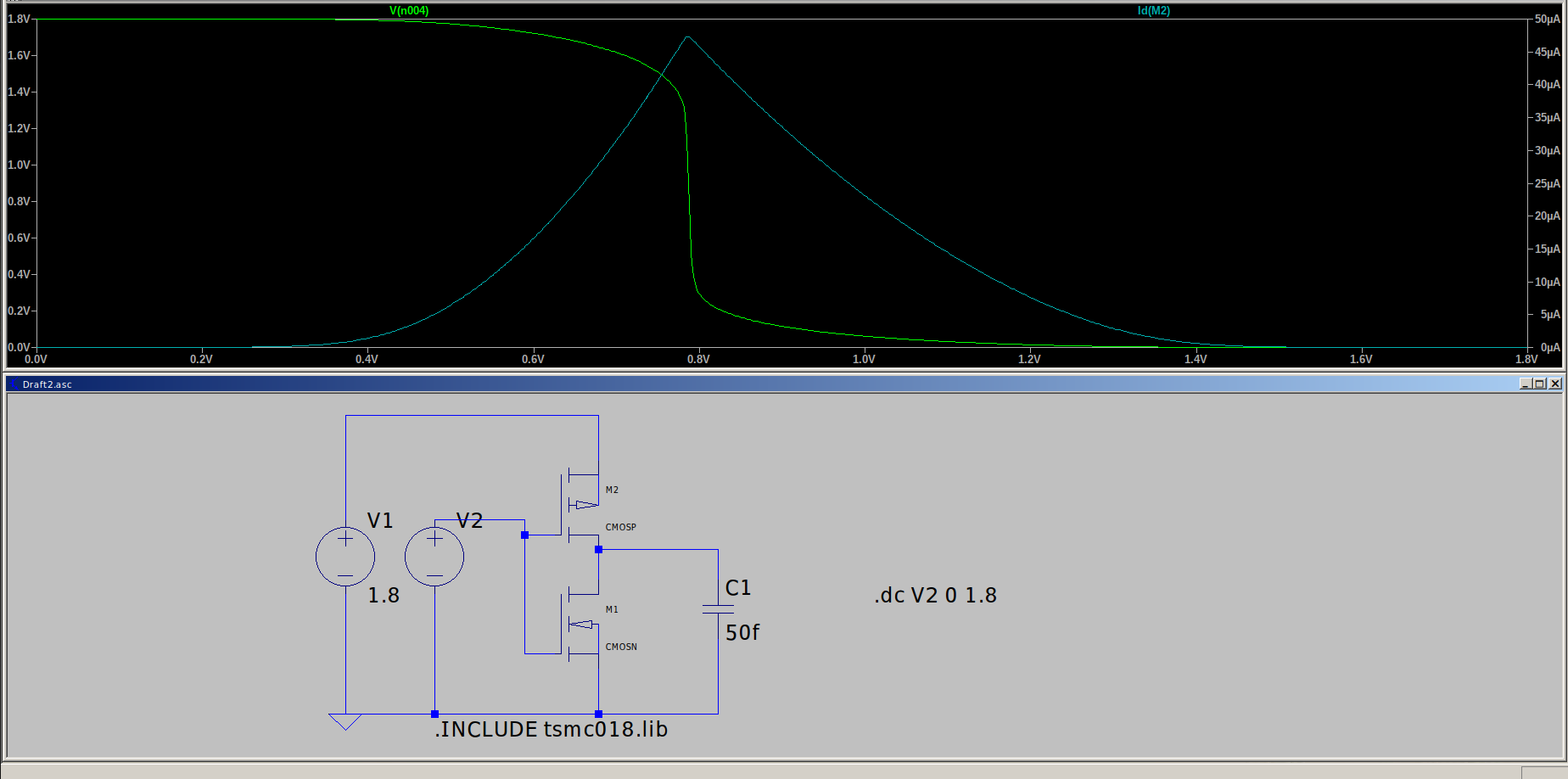
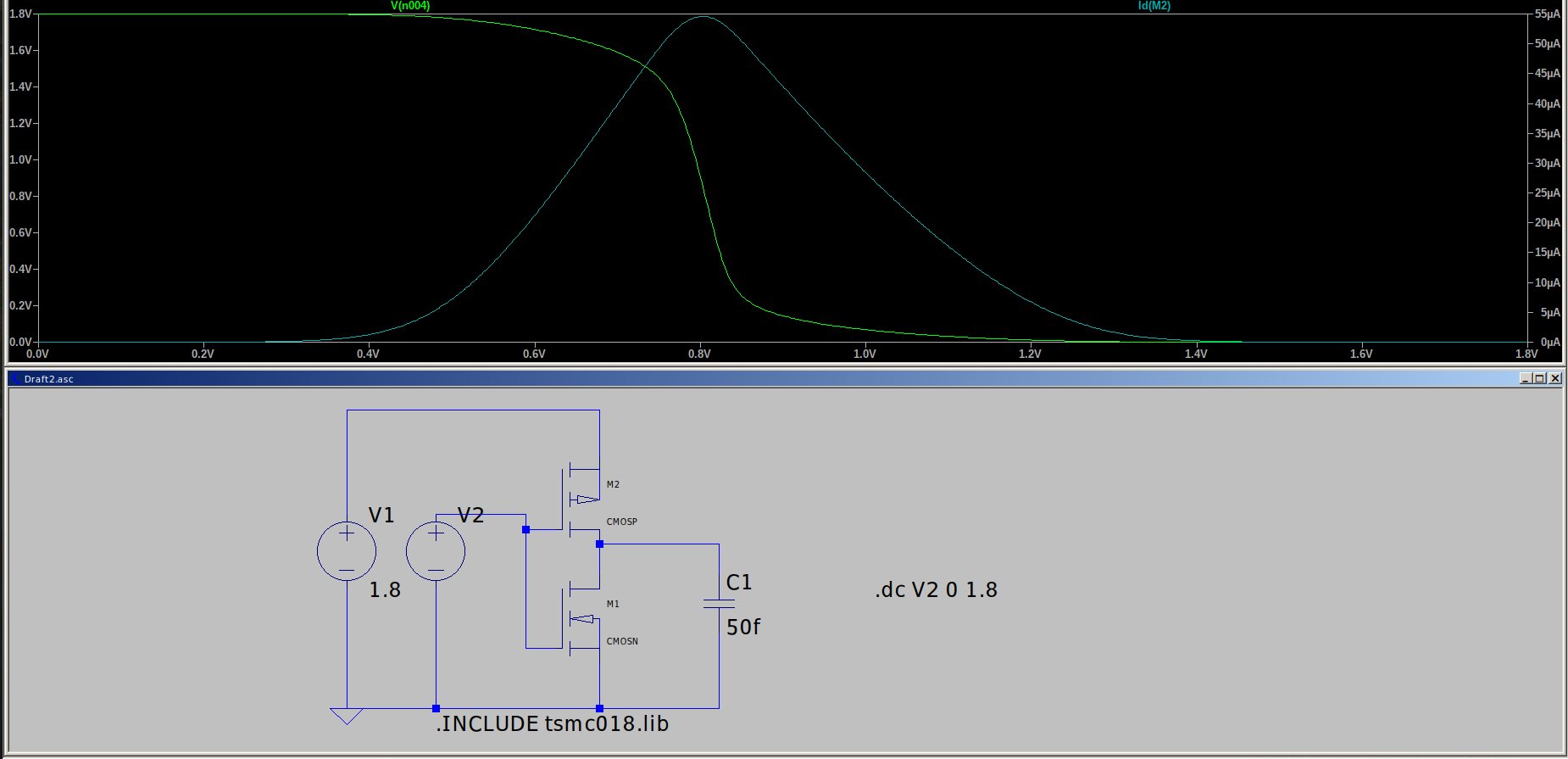
I am simulating the voltage transfer characteristic curve of a CMOS inverter, while varying the dimensions of L and W of MOS. Comparing the results for two scenarios, I have the following results:

Case 1:

  • Nmos L=180u, W=400u
  • Pmos L=180u, W=800u VTC has a very high gain at transition voltage.

Case 2:

  • Nmos L=180n, W=400n
  • Pmos L=180n, W=800n VTC has lower gain at transition voltage

For micrometer scale:

enter image description here

For nanometer scale:

enter image description here

Please explain the reduction of gain at smaller channel lengths in a CMOS inverter.

\$\endgroup\$
2
  • \$\begingroup\$ What is "gain"? Can it be read from that DC transfer curve you include? (yes it can, how?) \$\endgroup\$ Commented Dec 5, 2021 at 12:09
  • \$\begingroup\$ What do you understand about how changing the channel length and width changes the drain current? What happens if you change them such that the ratios of W:L and Wp:Wn are different? If you are not sure, ask your instructor. We won't do you homework for you. \$\endgroup\$ Commented Dec 5, 2021 at 13:23

1 Answer 1

3
\$\begingroup\$

The gain depends on the ratio of output impedance to gm of the MOSFETs. gm depends on W/L (at a given bias current), and is fundamentally quite similar for both circuits. However output impedance increases linearly with L, so is much higher for the longer devices; therefor the gain will be much higher.

Note that the large devices are extremely large, and will have HUGE input and output capacitances. That won't show up in your DC gain simulation, but in a transient simulation you will see additional C.dV/dt currents which will be quite large and may give confusing results. In addition, SPICE models for extremely long devices such as these are not accurate for this capacitance (search BSIM4 XPART) and will give inaccurate results for simulations where these capacitive effects are significant.

\$\endgroup\$
7
  • \$\begingroup\$ Thanks for your explanation. I am more concerned about dVout/dVin, rathar than actual gain. I think that this quantity must be independent of load capacitance. Can I think in terms of CLM as a reason for smaller dVout/dVin in nanometer scale ? Thanks \$\endgroup\$
    – Sparsh
    Commented Dec 5, 2021 at 19:41
  • \$\begingroup\$ @SparshSharma But gain is defined as dVout/dVin. In your case the signal frequency is very low but that doesn't change the fact that you are asking about gain. \$\endgroup\$ Commented Dec 5, 2021 at 20:30
  • \$\begingroup\$ His library is using a BSIM3 model with XPART=0.5 (i.e. 50/50 charge partition ratio). Which of the three partitioning schemes do you recommend for the transient simulation with these large devices? \$\endgroup\$
    – Ste Kulov
    Commented Dec 5, 2021 at 23:06
  • 1
    \$\begingroup\$ None is any good when switching FETs at a rate faster than the quasi-static approximation holds for. This can be approximated by the time constant or on-resistance * gate capacitance. If changing XPART gives different (transient and AC) simulation results, you know you have a problem. This is fundamental in the MOS model. You can mitigate in some cases by breaking a long FET into N shorter ones, each of length L/N \$\endgroup\$
    – jp314
    Commented Dec 5, 2021 at 23:14
  • 1
    \$\begingroup\$ Yes; there are all sorts of non-idealities in smaller FETs and nm technologies. Not only is there channel length modulation, but also DIBL (drain-induced barrier lowering) which also appears like an output impedance effect. \$\endgroup\$
    – jp314
    Commented Dec 9, 2021 at 15:59

Your Answer

By clicking “Post Your Answer”, you agree to our terms of service and acknowledge you have read our privacy policy.

Not the answer you're looking for? Browse other questions tagged or ask your own question.