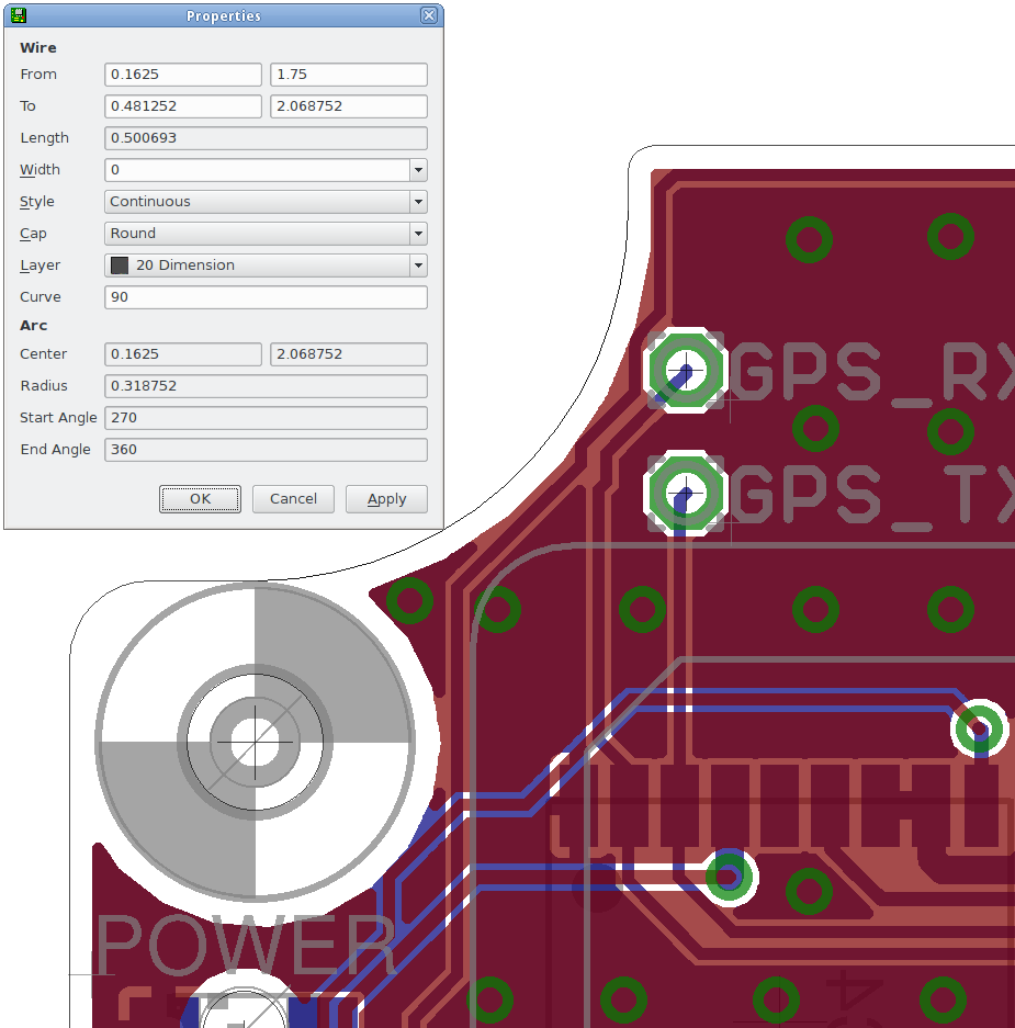
I've designed about 20 PCBs in Cadsoft Eagle, and for the board outline I've always used the "20 Dimension" layer, using "wires" of width 0 to enclose the PCB. I did this regardless of whether the PCB was rectangular (thus it could be separated from the panel by V-cuts), or non-rectangular (necessitating break routing).
As an example of non-rectangular PCB, see the part below. I've pressed "properties" on the long arc next to the dialog:

As you can see, the width is 0.
I've always assumed that
- A) the dimension defines what is the "inside" of your PCB shape, e.g. if you define your Dimension layer as a polygon (0", 0") -> (1", 0") -> (1", 1") -> (0", 1"), you should receive a PCB that is exactly 1-inch-sided square, differing up to manufacturing tolerances (and, importantly, the same size should be produced by either scoring or break routing)
- B) this definition is a bit abstract, and the PCB fab is expected to figure out the details. E.g., if they use 2mm break routing, they'd need to extend this shape by 1mm (essentially a Minkowski sum of my shape + 1mm circle) and that would give them the path for their router. They'd also need to figure out where to place the break tabs - it's not "my job" to select this. If they used 2.4mm break routing, they'd need to extend by 1.2mm. In any case, it seems wrong to assume what exact steps would the fab do to prepare my board for their manufacturing process.
In a debate with a coworker, he said my use of 0-width dimension is wrong, because the gerbers it generates are also a bit wrong, as e.g. CAM350 would complain about the zero width. One easy fix is to increase the width to e.g. 0.25", but this is not a no-op, as it actually shrinks the PCB a little. So in essence, he said I should fix my design by doing the Minkowski sum myself, using some non-zero width, if I wanted to get my PCBs the way I initially envisioned them.
I'm not convinced by his arguments, because
- the warning message could be just a peculiarity of CAM350
- I've sent at least 10 such designs to batching fabs like OSH Park and Ragworm, and I've never received a single complaint that my PCBs are not well-specified (but maybe they are lenient to noobs)
Questions
- Are my assumptions A & B correct?
- Is dimension of width 0 allowed / normal / accepted in the industry?
