10
\$\begingroup\$

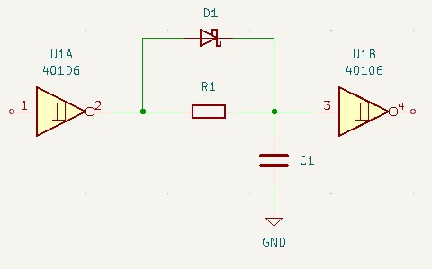
In designing a circuit, meant to delay only the rising edge of a square wave, I've got some doubts on determining the maximum value for C1 that can safely be driven by the CD40106 CMOS logic IC.

The discharging part of the cycle is no problem as that happens trough R1, but the charging is done directly trough D1 for as little delay as possible. I can't find any hard current-limits, maximum load capacitance or similar numbers in the datasheet.

How I think it's done:

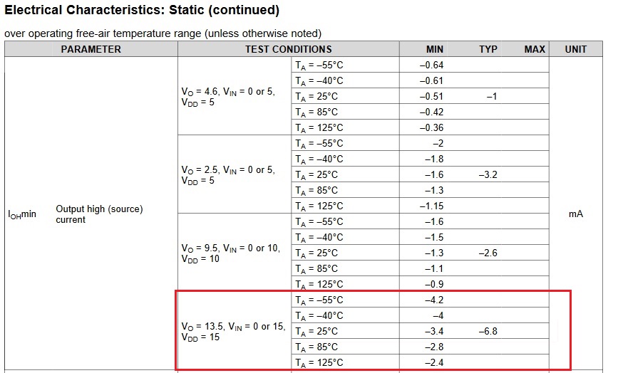
The datasheet lists some maximum power dissipation numbers for the whole device and per output-transistor, along with the available output current for a given output voltage and VCC:

So, a worst-case number of -2.4 mA @ 13.5V out for a 15 VCC implies a output resistance of:

$$\frac{15 V - 13.5V}{2.4mA} = 625 \Omega$$

One can then calculate the average power dissipated in 625 Ohm for a given C1 value and switching frequency and see if it does not exceed the maximum power dissipation numbers.

Is this method correct? Please detail the correct method if not.

\$\endgroup\$

4 Answers 4

4
\$\begingroup\$

CMOS 4000-series logic operating from 3-5V can sustain outputs continuously shorted to either supply rail. So capacitors don't really matter - they are just "poor" shorts.

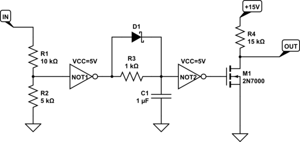
You don't need to use 15V VCC for RC circuitry, since it's meant to be slow, so you can drive the RC circuit from 3-5V, and use the output driver schmitt gate to drive an open-collector stage to step the voltage up to 15V:

schematic

simulate this circuit – Schematic created using CircuitLab

\$\endgroup\$
5
  • 5
    \$\begingroup\$ How would one arrive at the conclusion that continuous output shorts can be sustained at 3-5V from the datasheet ? \$\endgroup\$ Commented Oct 10, 2022 at 0:29
  • \$\begingroup\$ It is generally a good idea to add hysteresis to these types of circuits as the 'C' node slews slowly and can generate multiple transitions at the output. \$\endgroup\$
    – jp314
    Commented Oct 10, 2022 at 5:22
  • \$\begingroup\$ Weird. I used to toy with 4000-family logic gates for hobby/learning, exclusively at 5v, exclusively DC, no motors, flyback inductors, or boost circuits, etc. And I'm pretty sure I've burnt several such ICs. I can't provide schematics of what I did 10+ years ago, but hey, my circuits were SIMPLE like buttons and led blinkers and surely didn't exceed 5v at any point. \$\endgroup\$ Commented Oct 10, 2022 at 17:49
  • 2
    \$\begingroup\$ I searched a bit for anything that would support that claim, and I found something! wiki.analog.com/_media/university/courses/… page 3, quote "At lower supply voltages, certainly below VDD = 10V, the output resistance will be high enough that a single output may be short-circuited to either supply without exceeding the absolute maximum output current of 50 mA or the package dissipation of 500 mW. Short-circuits should be avoided when VDD > 10 V as either or both ratings may be exceeded. At VDD = 5 V, several outputs may be short-circuited without risk". \$\endgroup\$ Commented Oct 10, 2022 at 17:51
  • 2
    \$\begingroup\$ How would one arrive at the conclusion that continuous output shorts can be sustained at 3-5V from the datasheet? General experience with how much current these things deliver in practice vs. temperature. At least the CD4000 series from TI since that's what I've been using. Pretty much indestructible at 5V. The output drive at 5V is barely enough to overcome input capacitance and drive the inputs with a high enough slew rate. If you run CD4000 outputs at 5V at 1MHz, they are driving a short pretty much anyway, due to how long they slew. \$\endgroup\$ Commented Oct 11, 2022 at 0:04
8
\$\begingroup\$

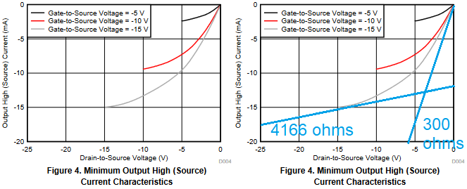
The output model envisioned is a rather simple linear one. The PMOS pull-up transistor has a voltage-current characteristic that is far less linear.
Pegging output resistance to one value is a less-than-accurate approach. Some insight to variations in equivalent output resistance might be gleaned from Texas Instrument CD40106B data sheet:
V/I graph from TI data sheet CD40106B of PMOS output driver

\$\endgroup\$
8
\$\begingroup\$

Rather than try to calculate and integrate I*V, you can consider that all the ½.C.V^2 energy required to charge the capacitor (ignoring the diode drops) comes from the output via the supply. Therefore the energy dissipated to charge the capacitor is also ½.C.V^2. Therefore you power is ½.C.V^2.f

CMOS ICs are no intended to operate at maximum power dissipation continuously, and there can't be a real guarantee of long term (years) reliability under this condition.

A better approach is to make U1B an OR-type gate; delete the diode, and drive the other input of the OR directly from U1A. Thus as U1A's output rises, the OR's output will rise immediately (even faster than your circuit); conversely when U1A falls, it will require the R.C to discharge and thus generate a delay.

This also has the advantage of dissipating most of the power in the resistor which can handle it reliably.

Instead of a Schmitt trigger, you can use a normal buffer (OR gate, not NOR gate), and add a small (say 10 % of C1) capacitor between input and output. This creates positive feedback with similar performance to a Schmitt trigger.

\$\endgroup\$
4
  • 2
    \$\begingroup\$ That amount of energy has to make it through the CMOS chip into the capacitor, but it's not necessarily dissipated (as heat) inside the chip. Unless the chip is the only resistance anywhere in the loop from power supply to ground, or nearly so. (e.g. capacitor ESR and other factors negligible vs. output resistance.) Then yes, since we know the cap won't charge instantly with infinite current, there was an RC time constant with the CMOS gate being most of the R. And it sounds about right that the integral of voltage drop x current across that R would be the capacitor energy. \$\endgroup\$ Commented Oct 10, 2022 at 4:17
  • \$\begingroup\$ that's nice. To avoid an extra IC you could also "diode OR" the output of the first gate and the top of C to do the same thing - one extra diode instead (probably same package if using SMD devices). You can also still have a low value resistor across the second diode which charges C quickly enough (whatever that means). \$\endgroup\$
    – danmcb
    Commented Oct 10, 2022 at 13:30
  • \$\begingroup\$ (update to previous comment: If the only resistance anywhere is in the CMOS gate, then yes. Charging from 0 to 5V is exactly like discharging a capacitor from -5V to 0 through a resistor; all the capacitor energy ends up as heat in the resistor.) \$\endgroup\$ Commented Oct 10, 2022 at 15:07
  • 2
    \$\begingroup\$ When you are using the diode to charge the cap, most of the enerfy is dissipated in the IC (you can ignore the ~ 0.3 V across the diode). When discharging, presumably the 1k ohm dominates and that portion of the energy is dissipated in the resistor. \$\endgroup\$
    – jp314
    Commented Oct 10, 2022 at 17:23
3
\$\begingroup\$

If I was really trying to charge that cap as quickly as possible, I would probably consider spending a couple of cents on an output drive transistor, to make things a bit more predictable and almost certainly faster.

However your phrase "as little delay as possible" leaves me with a feeling of incompleteness. There must be some minimum (1ns? 10ns? 100ns?) which is definitely tolerable and I would begin by trying to define that, otherwise it's rather hard to decide what is or is not a good solution.

With this kind of situation it also becomes important to know a bit more about your design objectives. Are you making one or ten thousand of these? (This would make me think about how much I trust those graphs of output characteristic to be reliably true for every chip in a big batch.) Is cost of extra parts a big deal (i.e. are you trying to shave every last cent off the cost?)

As I consider this circuit, I realise that there are two parameters at play here - the DELAY through the circuit (which you want to minimise) and the required PULSE WIDTH at the input to charge C fully and thus ensure that the delay is achieved. (A short pulse will cause incomplete charge and thus possibly a reduced delay.)

You could add one resistor and limit the charge current into C, while still having the output respond to the input with minimum delay. I think this helps your delay figures (as you now know the output voltage of the first stage will not be stuck low for a short period trying to charge the cap), at the expense of a longer (but well defined) input pulse to charge the cap fully. There is some dependence between pulse width and delay here, you may need to think about that (but there was before as well for very short pulses).

The values given here are notional, R1 sets the delay and R2 sets the minimum pulse width of the input that will cause the delay to take effect. For the values I give, the minimum pulse is around 20uS and the delay is about 0.5s (very approximate), of course you can adjust these to fit your application.
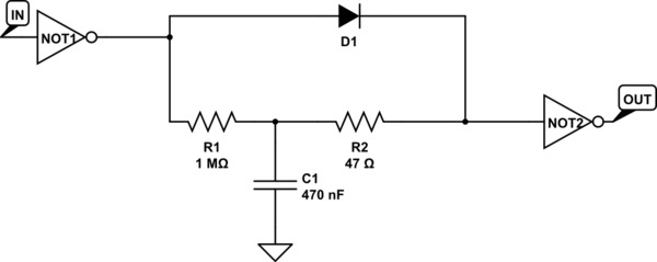
schematic

simulate this circuit – Schematic created using CircuitLab

\$\endgroup\$
2
  • \$\begingroup\$ I tought of this modification before asking the question but I asked it as is because I'd like to know how one calculates this using the datasheet. \$\endgroup\$ Commented Oct 10, 2022 at 14:53
  • \$\begingroup\$ I think you could do well to be a bit clearer about your design requirements. These logic chips aren't really designed to be operated into an effective short - even though they will likely survive it, it's just not good practice, and in the worst case you might see other unexpected effects. So the important questions are - how short does the delay really need to be, and how narrow might the input pulse be? \$\endgroup\$
    – danmcb
    Commented Oct 10, 2022 at 18:44

Your Answer

By clicking “Post Your Answer”, you agree to our terms of service and acknowledge you have read our privacy policy.

Not the answer you're looking for? Browse other questions tagged or ask your own question.