1
\$\begingroup\$

I understand that the basic idea is to construct a PUN such that \$V_f\$ (the output node) is raised up to \$V_{DD}\$ if and only if we have input valuations such that \$f = 1\$, and similarly to construct a PDN such that \$V_f\$ is pulled down to \$V_{SS}\$ if and only if we have input valuations such that \$f = 0\$. As far as I can tell, there are two cases, with my question regarding the second case:

  1. The given function \$f\$ has literals only in complemented form. In this case, things are easy and the PUN can be read off the function, with the PDN following from finding \$\overline{f}\$ which will be entirely in terms of uncomplemented variables. Thus we can again read off the PDN (and as expected it will be dual to the PUN).

  2. The given function \$f\$ has some literals in uncomplemented form. In this case, I am unsure how to proceed as the procedure of Case (1) does not work, at least a priori. For example, if I have a function like \$f = x_1 +x_2\overline{x_3}\$, how should I proceed? It's not clear to me how to "see" the PUN in the same way as in Case (1). What is the general strategy in such cases?

\$\endgroup\$
7
  • \$\begingroup\$ So case 1 is worded oddly to me - If I'm making a gate that implements the function \$\overline{Y}=A+BC\$, I can make both the PUN and PDN without compliments of the inputs. However, complementing one of the inputs or outputs would make the problem unsolvable if inverters or complementary inputs were not allowed. \$\endgroup\$
    – W5VO
    Commented Sep 29, 2023 at 17:39
  • \$\begingroup\$ Perhaps I am a bit confusing. For that function, I'd note that \$Y=\overline{A}(\overline{B} + \overline{C}) \$ which immediately gives me the PUN in terms of PMOSFET \$A\$ in series with the parallel combo of PMOSFETs \$B,C\$. @W5VO So yes, I am talking about the "mixed" case I guess. How does one proceed there? Perhaps I am misunderstanding your comment. \$\endgroup\$
    – EE18
    Commented Sep 29, 2023 at 17:51
  • \$\begingroup\$ I'm not following this question. Every pullup network of pfets has a complementary pulldown network of nfets, and the way to make things complementary is to turn stacked pmos into parallel nmos, and parallel pmos into stacked nmos. It doesn't matter if the literals are inverted or not--- if a literal needs to be inverted, and the same logic function is implemented in both NMOS and PMOS, then the literal needs to be inverted for both. The only exception would be using a different factorization in the PUN vs. PDN. \$\endgroup\$
    – stevesliva
    Commented Oct 2, 2023 at 1:15
  • \$\begingroup\$ I guess the point I'm trying to convey is that if I have a logic function $f$ wherein every literal is inverted (e.g. \$f = \overline{x}_1 + \overline{x}_2\overline{x}_3\$) then I can read the PUN immediately. I don't see how to read it if I have, for example, $f = x_1 + \overline{x}_2\overline{x}_3\$. Not sure if that makes my concern any clearer? @stevesliva \$\endgroup\$
    – EE18
    Commented Oct 2, 2023 at 22:37
  • \$\begingroup\$ @EE18 - you need an inverter for x1 in the 2nd case because the function doesn't have a factorization that results in a single gate. \$\endgroup\$
    – stevesliva
    Commented Oct 3, 2023 at 3:01

2 Answers 2

2
+50
\$\begingroup\$

In case 2, you could substitute \$y_3=\overline{x_3}\$. Drive the PUN/PDN with a complement as needed.

You could also complement the type of devices that would be taking the y signal, but that requires level shifting for the signal, and that adds quite a bit of delay vs an inverter.

But - PUNs and PDNs are not always the fastest implementations of a given logic function. Sometimes a ROM block is faster, especially as the number of inputs grows. So it all depends on the usual speed vs. energy use vs. area tradeoffs.

And anyway, the partitioning of branches of a PUN or PDN is by no means unique for a given logic equation, and there's no simple rule of thumb for speed vs size. Usually an optimizer gets to try all combinations, or explores a subset of design space using genetic programming, heuristics, simulated annealing, etc. This makes sense for PUNs and PDNs that are on the timing critical path.

\$\endgroup\$
3
  • \$\begingroup\$ Your comments re: the PUN and PDN being potentially suboptimal is well-taken, so I guess I'm just thinking of this as an academic exercise in that case. Would it be possible to see a diagram of what you're thinking about with respect to my \$f = x_1 +x_2\overline{x_3}\$ question? If it were \$f = \overline{x}_1 + \overline{x}_2 \overline{x_3}\$, then I could immediately see this as the PFET controlled by \$x_1\$ in parallel with the PFETs controlled by \$x_2,x_3\$ in series. But I can't "see" this in the other case, if that makes sense? \$\endgroup\$
    – EE18
    Commented Oct 2, 2023 at 22:41
  • \$\begingroup\$ @EE18 In modern chips, interconnect drives speed, and an inverter feeding a PUN or PDN element is free in terms of speed :) So, if you need not-x3: just make it with an inverter. You can always delay non-inverted signals with pass gates to make the edges all arrive at the same time to elements in both PUNS and PDNs. We’re talking picoseconds here though, even on processes from 2 decades ago. Sure if you go to 70s 4000-series CMOS process, or some modern biCMOS used for analog, an inverter is not free in terms of timing. But that’s not a concern in digital CMOS. \$\endgroup\$ Commented Oct 4, 2023 at 15:24
  • \$\begingroup\$ Understood, thank you! \$\endgroup\$
    – EE18
    Commented Oct 4, 2023 at 15:59
2
\$\begingroup\$

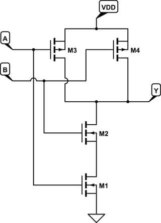
I think it would be helpful to consider simpler cases than a 3-input gate, and the rules for gate formation definitely hold up for 1-2 input static CMOS gates. It's just those gates often have names already. Consider the logic function to implement \$Y=\overline{A\cdot B}\$ which I have implemented as a "custom" logic gate below. The pull-up network consists of M3 and M4 in parallel, and is active when \$\overline{A+B}\$. The pull-down network consists of M1 and M2 in series, and is active when \$\overline{A \cdot B}\$.

schematic

simulate this circuit – Schematic created using CircuitLab

Some observations:

  1. The NFET pull-down network logical function matches the original function
  2. The PFET pull-up network does not require any logical inversions in the inputs (e.g. \$\overline{A}\$ or \$\overline{B}\$), only topological changes.
  3. The output function is always inverting.
  4. We don't really have a way of inverting an input in a single-stage gate like this. No inputs are inverted.

Observation 1 and 2 are pretty easy to follow, but we run up against 3 and 4 pretty regularly. So how do you implement logic functions like \$Y=A \cdot B\$ or even \$Y=A\cdot \overline{B}\$ in a single stage using static CMOS when you only have access to A and B? You can't.

When you have additional inversions that you can't work around, you must add an additional stage of logic to invert the signal.

schematic

simulate this circuit

\$\endgroup\$

Your Answer

By clicking “Post Your Answer”, you agree to our terms of service and acknowledge you have read our privacy policy.

Not the answer you're looking for? Browse other questions tagged or ask your own question.