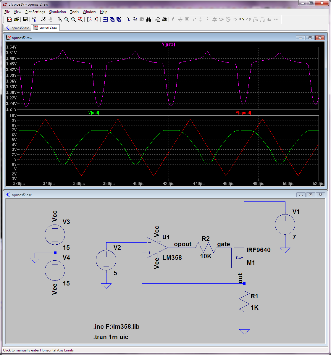
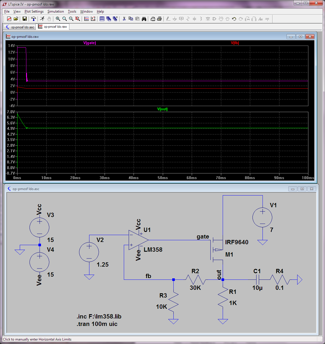
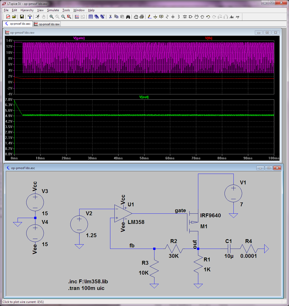
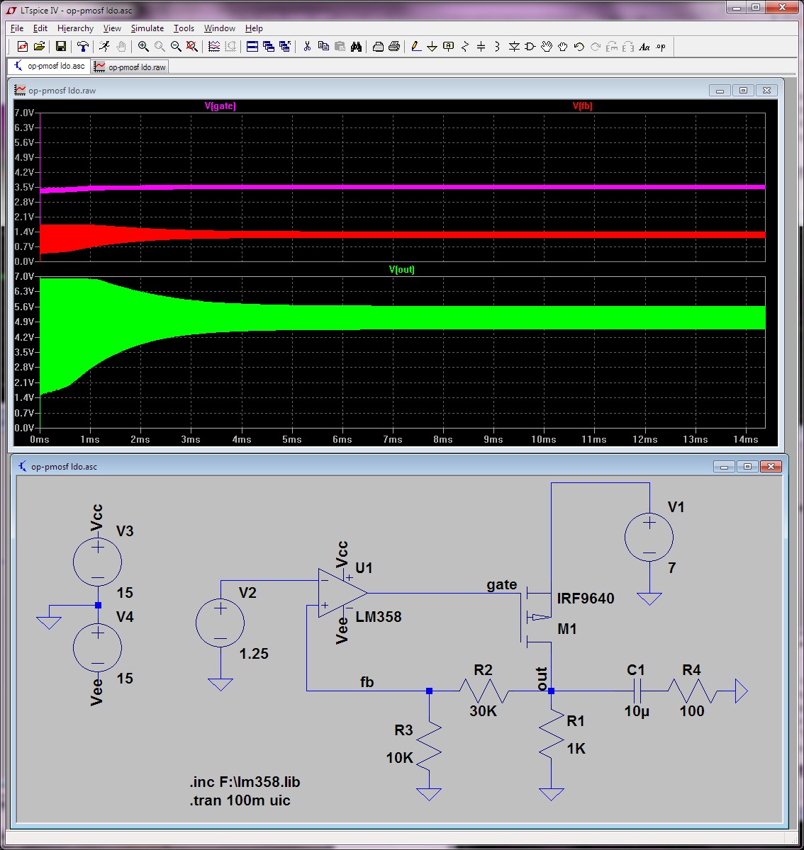
NOTE: This post has been extensively edited to add depth and clarity. While composing the original answer, a lot of details were considered that were not included to keep things brief. Here the skin is ripped off of the diagnostic and solution process to show what goes on under the surface and add substance. Think of it as a sort of diary of analysis. I'm leaving the original answer intact for transparent edits, adding detail in and after old text.
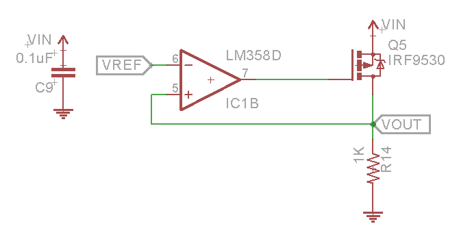
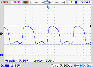
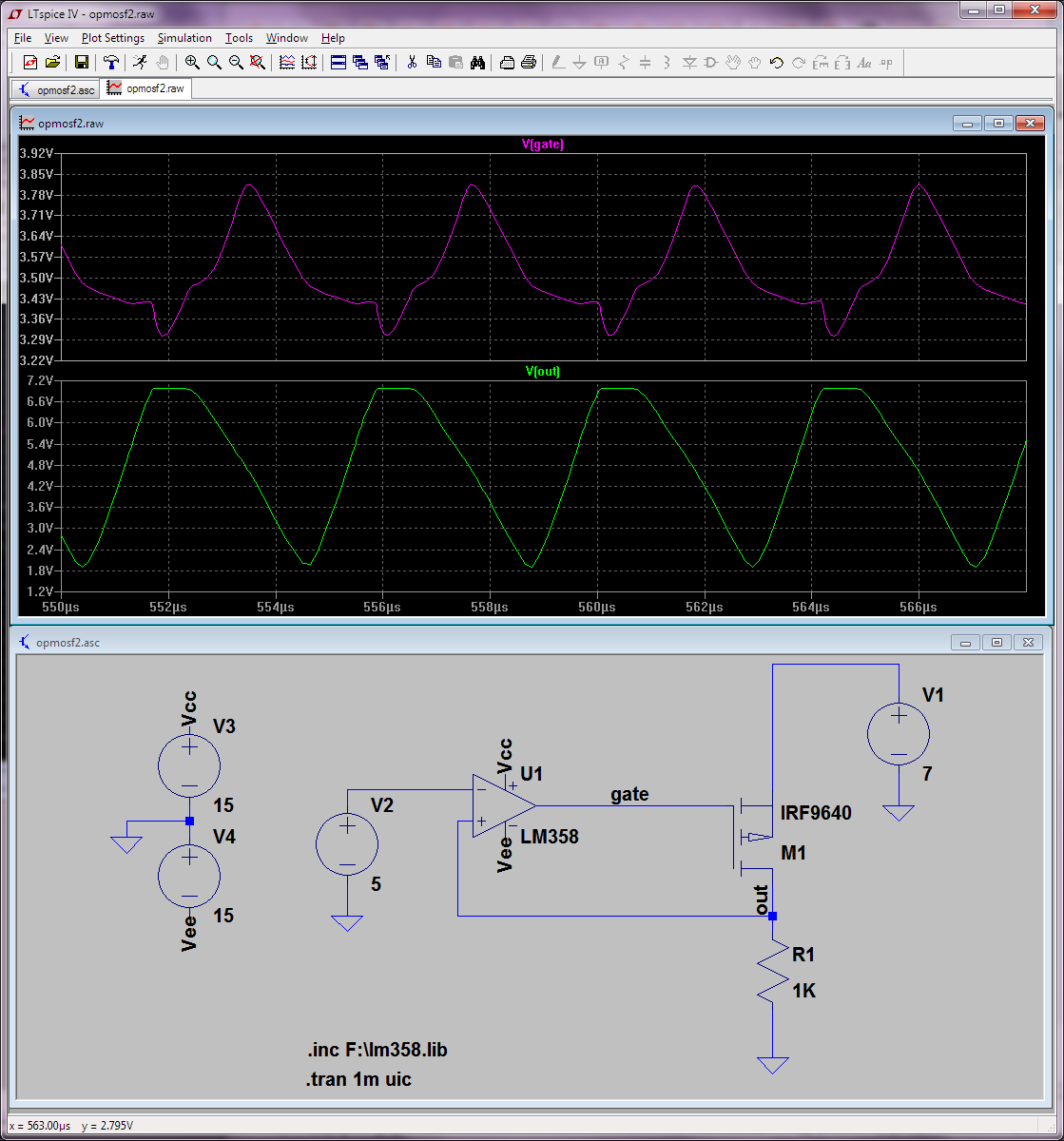
As has been pointed out, the output impedance of the LM358 is interacting with \$C_{\text{iss}}\$ of the FET to place a pole at about 20kHz. Since the loop still has lots of gain there it oscillates.
Editorial commentary about the diagnostic:
Where does this 20kHz pole come from?
It is not from \$C_{\text{gs}}\$, because that pole will not show up until in the MHz. This is a common source amplifier with resistive load (\$R_{\text{14}}\$ in the drain and resistance in the gate circuit (call it \$R_g\$). Location of the dominant pole for this sort of amplifier is approximately:
\$F_p\$ ~ \$\frac{1}{\text{2$\pi $} R_{14} C_{\text{gd}} g_{\text{fs}} R_g}\$ ~ \$\frac{1}{\text{2$\pi $} \text{(1000)} \text{(150pF)} \text{(5)}\text{(10)}}\$ ~ 21.2kHz (close enough)
So, the pole comes from \$C_{\text{gd}}\$ the Miller capacitance, which is so important here as it is multiplied by FET transconductance (\$g_{\text{fs}}\$) and load resistance (\$R_{\text{14}}\$). Do a quick sum of loop phase shift to see that, best case, you would expect 45 degrees of phase margin left at 20kHz (LM358 -90, IRF9530 -180 -45 = -315 degrees). Already, at 20kHz, phase margin is at best the minimum you would ever want to see in your loop, being 45 degrees and it's probably less than that. OK, so far this is a total SWAG. Its scientific since I used a scientific calculator to multiply and divide, and its a wild guess since I haven't yet looked at the datasheet for the IRF9530, and haven't refreshed my memory of the LM358 Zo. It does give a quick indicator of likely source of problem for the OPs circuit.
Looking for the most simple ideas to improve the situation:
First tried to provide a simple solution for the original circuit, resulting in the two bulleted statements below. These are both band-aid approaches that can't be taken far enough to make any meaningful difference. The lesson here (that I should already know) is never provide band-aid solutions, since they are not worthwhile. There are of course ways to fix the original approach, but they are more fundamental and complicated.
Then (finally) I suggested a source follower based circuit as a place to start as a solution. This idea is sound, including the integrator cap and FET \$V_{\text{th}}\$ caveat. I'll show why this is true in the next editorial comment after the source follower schematic.
A couple of notes about the circuit I suggested:
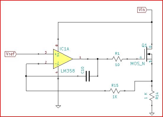
R1 in series with the gate is just a convenience. It is very common in circuits like this to need to isolate the gate for troubleshooting or testing. Popping up a resistor is a 5 second operation. Lifting the lead of a TO-220 is much less convenient, do it more that a couple of times and you may even lift a pad. If you are using a surface mount part, with out the resistor you will be having to remove the FET.
I show a 1kOhm resistor for R15. Really though, considering the output impedance of the LM358, I would not use anything less than 10kOhm ... and might even go as high as 50kOhm.
You could try:
- Lowering the output impedance of the amplifier (a lot) by adding an emitter follower buffer at the amp output.
- Isolate the \$C_{\text{iss}}\$ of the FET by putting some resistance in series with the FET source (between the FET and Vin. This would be kind of a band-aid approach.
Since the + input of the amp is being used as the negative feedback point, you have complicated things. Normally you would want to use the OpAmp as an integrator with a feedback capacitor from OpAmp output to - input. That way you could control the amplifier crossover point so that the phase loss caused by the FET capacitance could be unimportant or compensated for.
You might start with something like this:

Choose a value for C10 that causes amplifier gain to cross zero gain at 1kHz or less for stability. Using a FET you won't be able to get more than about 3V with any load at the output. In which case you would have to look at using a BJT or higher Vin.
Editorial commentary about the source follower solution:
Here is how I thought about a basic design solution.
What do we know about what svilches is trying to do with his circuit? Well, he wants to use 7V to provide up to 5V with up to a 1 amp load, and he wants to have the output voltage track a control voltage (that he calls a reference voltage). Basically, wants a linear adjustable power supply using a LM358 opamp for loop error compensation and there is only 2 volts of head room (that will be a problem for the LM358).
We don't know what kind of modulation will control the reference. Will it be a ramp, a sine, or maybe a pulse or step modulation? Step is the worst, although if you plan for it is not that big a deal, so figure the reference input moves in steps.
We don't know much about the load either. Is it steady current, or pulsed? Well, svilches is vague about it ... just needs up to 1 amp. But usually, ill defined loads are not steady, so I'm going to expect pulses here too. Also, since this is a power supply I am surprised to see no output capacitance (\$C_o\$) in the circuit ... but we'll cover that later.
Two basic ways to go:
Either compensate the common source circuit to be stable, or switch to a source follower circuit. The first option has a lot of merit, but is more complicated and I was looking for the fastest and least complicated solution. Second option, the source follower is a simpler design because it is constrained. By constrained I mean changing from a pass element that buffers current and has voltage gain to one that buffers current and has (except for special circumstance defined by parasitic elements) unity voltage gain. The advantage of the common source circuit is that it is a low drop solution, which you loose with a source follower amplifier. So, the simple place to start is the source follower.
Problems using a source follower power stage here:
- Only 2V of head room means a really low \$V_{\text{th}}\$ FET. Also, with \$V_{\text{ds}}\$ of 2V and current less than 1A, \$g_{\text{fs}}\$ will be low and \$C_{\text{gd}}\$ will be high.
- Using a LM358. The output of the LM358 has problems, output impedance is high and doesn't handle capacitive loading well (I'll cover this a lot more in a bit). Also, the output of the LM358 won't get any closer than 1.2V to the 7V rail, leaving only 0.8V for FET \$V_{\text{gs}}\$ (take a look at Fig 10. of the LM358 datasheet to see that this is true). As I pointed out originally, don't expect more than 3V at the source of a standard FET with this circuit. Don't get too excited about using a BJT either because at 5mA into the base the maximum output from the OpAmp will be 5.6V, so a \$\beta\$ of at least 200 will be needed and that's with \$V_{\text{ce}}\$ of 2V. That P channel power stage is looking better all the time, but we'll keep going with the source follower. Side note about the LM358: National Semiconductor liked this amplifier enough to put it into at least 3 product lines LM124 (a quad) LM158 (a dual) and LM611 (a single with reference). Datasheets for the LM124 and LM158 aren't too clear about performance near crossover, but the LM611 datasheet is great ... see especially figures 29, 30, 35, and 36. Oh, and while you are at the LM611 datasheet, have a look at those example circuits that have integrator caps around the OpAmp.
To save time and keep things moving lets pretend that \$V_{\text{th}}\$ is OK and use a compliment to the IRF9530, the IRF520 as a model pass element.
From the datasheet for the IRF520 we see for \$V_{\text{ds}}\$ of 2V current about 1A that \$g_{\text{fs}}\$ ~ 1 and \$C_{\text{gd}}\$ ~ 150pF. Now, one of the benefits of the source follower amplifier is that is gets rid of \$C_{\text{gs}}\$ loading that the OpAmp will see (at least until capacitive loading is added to the source ... then it's a different story). It's \$C_{\text{gd}}\$ you need to be aware of.
\$C_{\text{gd}}\$ still provides direct loading of 150pF (for the IRF520) to the OpAmp output, an OpAmp which is already having trouble with 50pF. Take a look at Fig 8 of the LM358 datasheet. There you will see small signal voltage follower pulsed response of the LM358 with 50pF load. It shows an overshoot of 1.3 times the step input, and that means that the phase margin of the amplifier is 45 degrees.
When gain falls at 20dB/decade phase is 90 degrees if the nearest simple pole is a decade away. A simple pole will cause 90 degrees of phase shift over 2 decades centered with 45 degrees of shift at the pole.
So, effectively, there is a pole at the crossover frequency if the amplifier has a 50pF load. This is probably a combination of the pole caused by amplifier output impedance and capacitance, and the higher frequency poles that exist in the amplifier response that add up to contribute the extra phase shift. It doesn't matter though how all the phase shift got there, what matters is that some of it is directly attributed to the pole caused by amplifier output impedance and capacitive loading. 45 degrees with 50pF of load. But, \$C_{\text{gd}}\$ is 150pF, which will push the effective pole frequency back by about 1.5 octaves (1.6 octaves really, but why quibble over 0.1 octaves). 1.5 octaves is worth about 20 degrees of phase shift, so now the amplifier has only 25 degrees of phase margin. If 45 degrees of phase margin results in overshoot of 1.3 how much overshoot would be expected with 25 degrees of phase margin?
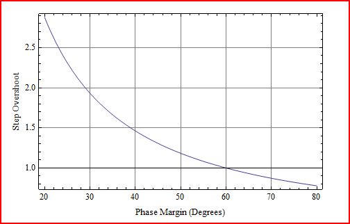
Here is a plot of step overshoot versus open loop phase margin for a unity gain unity feedback amplifier.

Locate 25 degrees of phase margin in the plot and see that it matches an overshoot of about 2.3. For this source follower circuit using a IRF520, you would expect a step input of 100mV at the reference voltage to cause an overshoot of 230mV on top of its 100mV response. That overshoot would turn into ringing at about 500kHz for an extended period. A current pulse on the output would have a similar effect of big overshoot followed by ringing at about 500kHz. This would be unacceptably lousy performance for most people.
How could all that ringing be reduced? Increase the phase margin. The easiest way to increase the phase margin is to add an integrator cap around the amplifier inside the unity feedback loop. Phase margin greater than 60 degrees would eliminate ringing, and you can get this by reducing Opamp gain by about 6dB.
A Likely Scenario
Recall that this is basically a power supply. Here is a likely scenario, if the source follower is built without an integrator cap. There will be some disturbance or pulsing on the output, and the circuit will ring. The user won't like that and will add some capacitance to the source. Maybe just 0.1uF. As capacitance loading is added to the source of the FET, gfs (low anyway because of low \$V_{\text{ds}}\$) will lose the ability to cover up \$C_{\text{gs}}\$. Capacitive load at the Opamp output will start to increase from 150pF, moving towards 500pF. The ringing with added capacitance at the source will get worse. The user won't like that either, and will try even more capacitance to load the source. By the time capacitance at the source has reached 1uF, the circuit most likely will no longer ring ... it will oscillate.
Since I expect capacitance to be added to the output of the circuit, I would size the integrator cap to lower the loop gain by 20dB or so.
