1
\$\begingroup\$

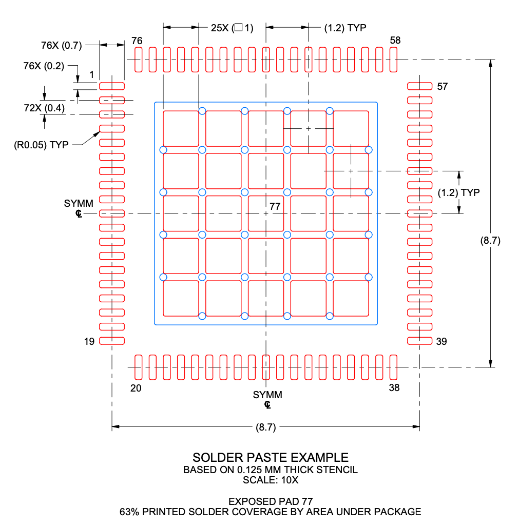
If a VQFN package (below) has a thermal pad and thermal vias beneath it, the bottom layer should have an identical pad to act as a heat sink.

Is it typical to surface mount a heatsink on the bottom-side thermal pad, over the thermal vias, (assumably using plugged and capped vias)?

enter image description here

Linked question: IC thermal pad: Duplicate zone in inner layers also?

\$\endgroup\$
3
  • 1
    \$\begingroup\$ Do you have a bottom pad and holes that can hold a heatsink? Usually it is not recommended to solder parts on the bottom layer of a QFN footprint, but it can be done. \$\endgroup\$
    – Lior Bilia
    Commented Feb 14 at 16:06
  • \$\begingroup\$ If you plan on mounting a heatsink, isn't the simpler solution to mount it to the top of your package? Even though the thermal conductivity may not be as good, would it not be adequate? Using internal and bottom layers will likely help (there are calculators for that...), and I see no reason why the shapes on the other layers would need to (or want to) be the same shape as your paste layer (usually, the larger, the better). \$\endgroup\$ Commented Feb 14 at 16:45
  • \$\begingroup\$ I would look around for either additional information in the layout section of the datasheet or maybe an app note from the manufacturer. Mounting a heatsink on the opposite side of the board does not sound like something the manufacturer would expect you to do without further guidance. \$\endgroup\$
    – vir
    Commented Feb 14 at 16:49

3 Answers 3

1
\$\begingroup\$

Common, I don't think I would say so. "Viable", yes.

QFNs tend to have reasonable thermal performance through the top (packaging plastic is a pretty mediocre thermal conductor, but it's thin), so you see gap pads on top of them, from time to time.

Bottom is less common I would say, in part because once the heat is into the board, it spreads out reasonably effectively into the inner layers. First, if inner-top is GND, the plane spreads out heat by direct conduction; in combination with the bottom pour (if applicable; it doesn't need to be an "identical pad", it can be any random solder-masked polygon, or left off entirely if not required), the inner-bottom layer (usually VCC plane) is sandwiched, so has excellent thermal conductivity as well; or perhaps you're using a sig-GND-GND-sig stackup instead and both planes are directly connected. And needless to say, multiier-layer boards are even more conductive, regardless of plane assignment.

Thus, the board itself is an effective heatsink, and I would not at all mind running a device such as pictured, up to several watts, in an otherwise very ordinary build (normal commercial sort of product, no stringent limits on ambient or device temperature, single board much larger than the chip, still air or minor ventilation).

A very compact design, or with tighter temperature specs (say an ambient up to 60°C with a chip limit of 85°C), or higher power levels (5, 10W might be the practical limit here), would benefit from thermal pads top and bottom. Such a heatsinking solution will be more onerous, as you most likely can't simply place elements at will, but must integrate them into the design. Pretty quickly beyond here, one would run into package limits, and a device with exposed metal/die surface would be required, with a greased joint or high-K gap pad to heatsink/heat pipe. Such packages are common in computing: advanced integrated regulators, CPUs/GPUs, etc. Heat sunk through the board again becomes less important then; so, it's kind of a narrow range (of ratings or products) where this approach would be preferable.

\$\endgroup\$
2
\$\begingroup\$

If a VQFN package (below) has a thermal pad and thermal vias beneath it, the bottom layer should have an identical pad to act as a heat sink.

When you say bottom layer I'm assuming you mean the bottom layer of the PCB?

The answer depends on where your ultimate heat sink is. For instance, if your PCB is conductively cooled through the edges (edge rails) of the board, then a thermal pad under the PCB is not going to do anything for you.

On the other hand, if your PCB is going to be attached to a solid aluminum heat sink, then a thermal pad on the bottom side of the PCB under the VQFN package, or under the entire PCB (which is typically the way we would do it) would improve the thermal path from the part to the heat sink.

\$\endgroup\$
1
\$\begingroup\$

Yes. (When there is a thermal pad in the center of course). Multiple vias can be drilled over a grid covering the thermal pad. To fix the heatsink on the other side, four holes (or at least two) should be drilled with enough free area on both sides around it for blots and screw heads.

It should be specified to the fab that they are "filled vias". Vias that will be filled with solder during assembly. Usually they just let the via being filled naturally by the solder on the pad and it doesn't involve any additional process.

A lot of small diameter vias are a little bit better than a few large diameter vias. But if the supplier doesn't like small diameters, larger diameters are still ok.

If the heat is not very strong, an extended uncovered copper area can be enough to act as a heatsink.

\$\endgroup\$

Your Answer

By clicking “Post Your Answer”, you agree to our terms of service and acknowledge you have read our privacy policy.

Not the answer you're looking for? Browse other questions tagged or ask your own question.