4
\$\begingroup\$

I have a push-pull converter that uses BSC040N10NS5ATMA1 MOSFETs. I have also tried using CSD19533Q5A MOSFETs.

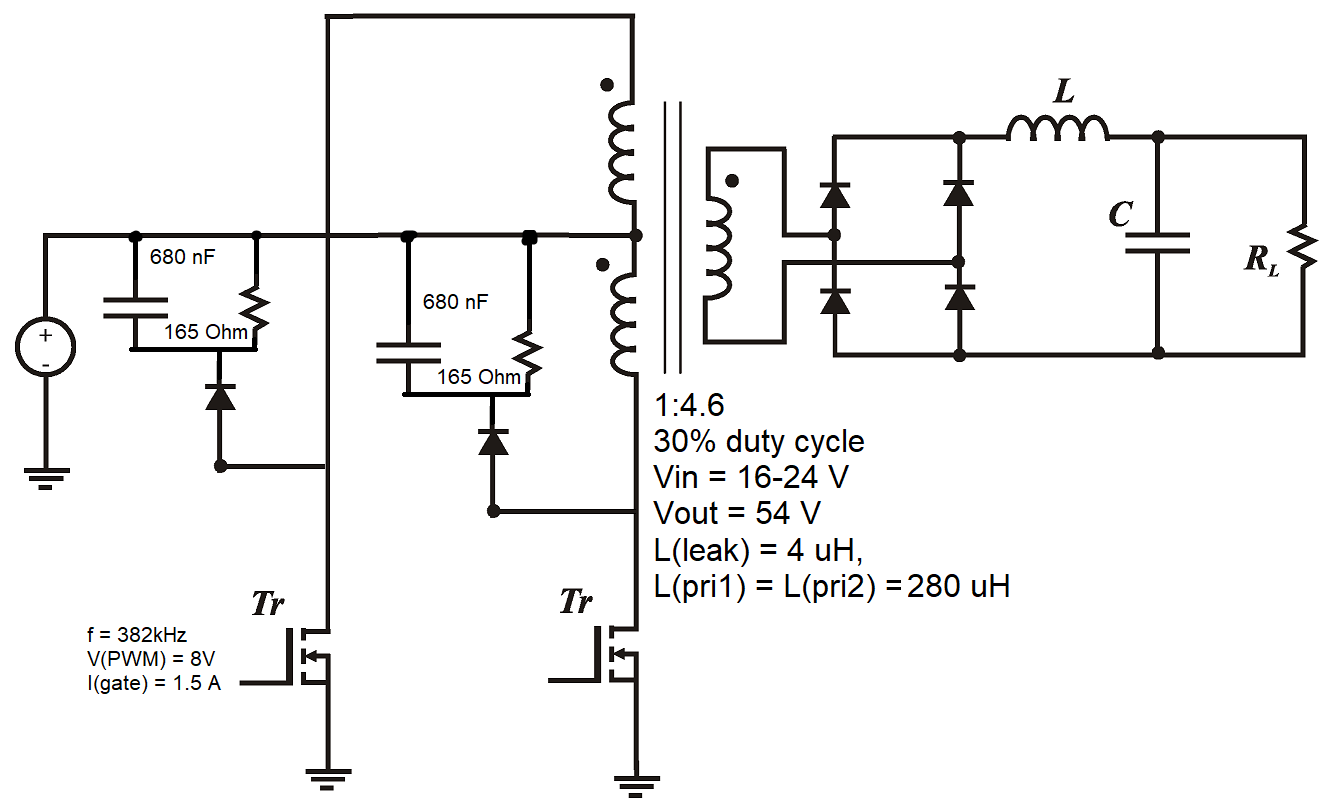
The FETs keep blowing at low power output (about 15 W). I am trying to get to 100 W. They fail to a short circuit. When I replace a FET, it happens again. Here is my circuit:

enter image description here

Things I have tried and verified:

  • Gate-source resistor: currently set to 10 kΩ
  • Gate drive resistor: currently set to 1 Ω, have used as high as 3 Ω
  • The duty cycle, turn-on time, and frequency are such that the gate voltage waveforms are not overlapping, so I do not think cross-conduction is the problem. Acutal duty cycle is still a bit higher than design duty cycle (40% vs. 30%), but the waveforms do not appear to overlap and the driver adds in about 40 ns of dead time.
  • The diodes in the snubber are very fast, part number UF4004.
  • I cranked up the gate drive and current as shown in the circuit and I am pretty sure I am fully turning on the MOSFET.
  • I also tried to use the FETs in parallel to reduce current per FET, and made sure to apply parallel gate driving, I see the same problem at the same power level (about 15 W)

I think the problem is that my resistor in the RCD snubber is wrong, but I don't know if it is too large or too small.

Any ideas?

EDIT 1: Inductance measurement

Leakage inductance is high actually about 4 μH, Primary inductance is actually 280 μH, turns ratio is accurate. Edited in image above.

EDIT 2: V(DS) and V(GS) measurements

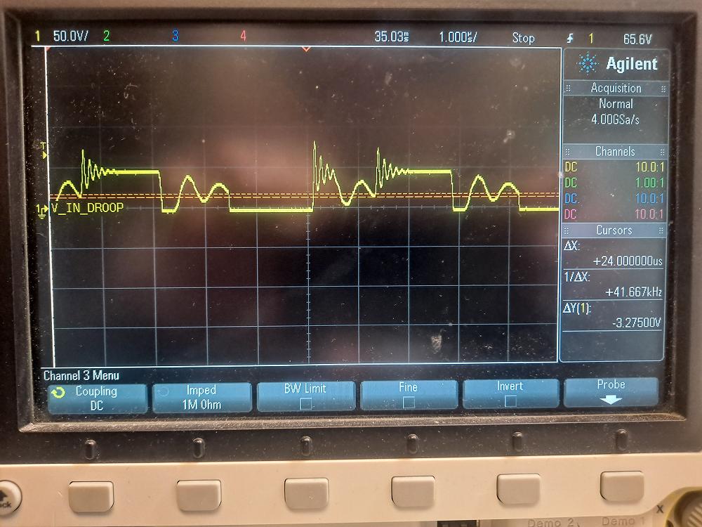
Initially I measured V(DS) using the RCD clamp values above, and I saw that V(DS) was spiking above 100 V at 15 W output, which is beyond the allowed value for the BSC040N10NS5ATMA1.

I changed the snubber values in the hopes that this would clamp V(DS). My measurement with C in the clamp replaced with 6.8 nF is shown in the photo. This was also taken at 15 W.

V(DS) is getting pretty close to 100 V. Also R in my RCD clamp was getting so hot that it looked like it was desoldering itself. A measurement of the capacitor shows that it completely discharges and rings during each cycle due to the low time constant.

enter image description here

V(GS) was a nice clean square wave on both MOSFETs with no ringing, found to be about 50 ns rise time.

\$\endgroup\$
8
  • \$\begingroup\$ Core could be flux walking into saturation, or drain could be ringing above VDS max. \$\endgroup\$
    – John D
    Commented Feb 27 at 17:38
  • \$\begingroup\$ Is your circuit correct, with the second RCD clamp going to the other drain? The leakage is quite high, what margin do you supposedly have between the voltage on the drain and the \$BV_{DSS}\$ of the MOSFETs? I remember often seeing TVS there or \$RC\$ snubber like in this doc from Nat Semi. Check this answer on SE also. \$\endgroup\$ Commented Feb 27 at 17:40
  • \$\begingroup\$ Are you sure the schematic is drawn correctly? What is the leakage between primary halves? \$\endgroup\$ Commented Feb 27 at 17:41
  • \$\begingroup\$ My mistake on the MS paint schematic, I updated it \$\endgroup\$
    – user224284
    Commented Feb 27 at 17:44
  • \$\begingroup\$ @JohnD if the drain is ringing above VDS max that would translate to an 80V ringing amplitude! Those BSC FETs have a 100 V maximum VDS spec. I'm really hesitant to think that is the cause. \$\endgroup\$
    – user224284
    Commented Feb 27 at 17:45

3 Answers 3

2
\$\begingroup\$

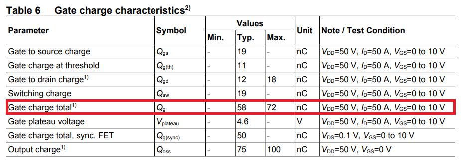
If we take the BSC040N10NS5ATM as an example. The total gate charge figure could be as high as 72 nC. If we divide this by the gate voltage specified in that parameter (10 volts), we get an effective gate-source capacitance of 7.2 nF. I follow this route to calculate capacitance because it takes into account a lot of the dynamics when operating as a switch. Image from data sheet: -

enter image description here

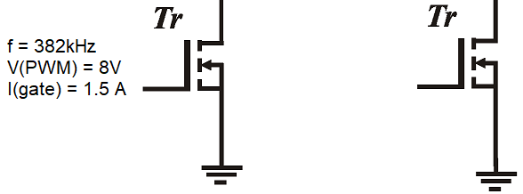
So now we have a way of calculating the turn on time of the MOSFET when the driver voltage is 8 volts and the driver current is limited to 1.5 amps. I use the capacitor equation \$I = C\frac{dv}{dt}\$ and 1.5 amps divided by 7.2 nF is a rise time of 208 mV per nanosecond. You are driving it at 8 volts hence, the rise time will be at least 38.4 ns. The fall time will also be 38.4 ns.

enter image description here

You are switching at 382 kHz, a period of 2.62 μs and, if running at 45% duty, the on time duration would be 1180 ns and your rise and fall times represent 6.5% of the period. This seems a little high to me given that the turn on time for the MOSFET can be as low as 9 ns.

I think you need to look at this and determine whether the peak power dissipation in the rise/fall periods exceeds an acceptable limit. You can do this using a simulator of course (and you don't need any fancy MOSFET models to do this).

You should also check the other MOSFET you have used following the same procedure as above.

\$\endgroup\$
4
  • \$\begingroup\$ I added V(DS) measurement above. How exactly would I "determine whether the peak power dissipation in the rise/fall periods exceeds an acceptable limit" ? What is the acceptable limit and what would I be simulating? Is this power dissipation given by (drain current)*(Vds) during turn-on? \$\endgroup\$
    – user224284
    Commented Feb 28 at 4:29
  • \$\begingroup\$ @sparaps do you use a simulator? Which one? How often do you simulate? \$\endgroup\$
    – Andy aka
    Commented Feb 28 at 8:57
  • \$\begingroup\$ I use LTspice and sometimes PSpice but I've never done this type of FET simulation. I'm not sure where to put probes or what I need to measure. Also assuming that the FETs are dissipating too much power during turn-on, what is the solution? \$\endgroup\$
    – user224284
    Commented Feb 28 at 17:24
  • \$\begingroup\$ @sparaps I would genuinely start a new formal question about this and open this up to the full crowd on here. If the MOSFETs are dissipating too much power then I'd certainly look at using a much faster driver circuit. The same power will be dissipated but, for a shorter time and that might bring some joy when you look at the safe operating area curve in the data sheet. \$\endgroup\$
    – Andy aka
    Commented Feb 28 at 18:09
2
\$\begingroup\$

A drain source short is a likely consequence of drain-source breakdown. The current limit of your DC supply then prevents excessive power dissipation/fire/smoke, so all you see is that it stops working.

In contrast, slow switching, or gate ringing or shoot-thru all cause massive dissipation in the MOSFETs, while leaving the DC current draw almost untouched. So these typically cause smoke and FETs blowing up.

4 uH leakage inductance is huge indeed, so it is very likely, IMO that hard switching with this transformer will always be challenging due to the very large drain-source-voltage spikes.

Energy in the leakage inductance at 1 A, is roughly 2 uJ. At 300 kHz this becomes 1.2 W of power to shove away, half of that in each snubber. The snubber resistors must be such that at this dissipation, they drop low enough voltage to remain well below 100 V. And of course they must be able to handle the dissipation. If you notice that they start melting solder, then this is not the case. If the solder joint becomes unreliable for even a ms, the snubber voltage would surge to extreme levels.

Moreover, snubber energy scales with current squared. So at 5 A, that already becomes 30 W, or 30% of your design power.

Without current mode control (do you have that?), on-time asymmetries will make the core saturate, so that means even more flyback energy.

\$\endgroup\$
2
\$\begingroup\$

Here is "another" way than "snubbers".
Used a "triangle" of capacitors at the primary side.

The max power with the values of your components is approximately 30 W.
Efficiency is about "97 %". Edit : perhaps "92 %".
Changed MOSFETs. Don't have yours in my database.

enter image description here

enter image description here

Added:
After "some" changes and "adding" ...

enter image description here

Here is an example of "supplemental" diode (one closed and one open) ...

enter image description here

\$\endgroup\$
1
  • \$\begingroup\$ There are many hidden assumptions in this answer. If you switch not at the valley point, efficiency will plummet, and the caps will just create more heat in FETs. In your last sim with included drain inductance, you should probe Vd between this inductance and the actual MOSFET. \$\endgroup\$
    – tobalt
    Commented Mar 7 at 18:47

Your Answer

By clicking “Post Your Answer”, you agree to our terms of service and acknowledge you have read our privacy policy.