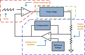
It will help to look at what an error amplifier actually looks like, and what that "compensation" block is: https://www.ti.com/lit/an/slva662/slva662.pdf.
The above link is for the TI article "Demystifying Type 2 and Type 3 Compensators".
I won't go into the differences between, type 1,2 and 3, but you'll see a common theme. There is no DC path in the compensation. It is all capacitors. The goal of any op-amp is to get it's inputs to be equal. In the case of an SMPS Error Amplifier, this means that the scaled representation of the output voltage is equal to the reference voltage shown in your image.
Like you pointed out: different loads, different inputs, different outputs, etc, all require different duty cycles to maintain. Duty Cycle is set by the output of your EA. The EA output is compared against a sawtooth, so a higher EA gives a higher duty cycle and a lower EA value gives a lower duty cycle.
To understand how EAs work, lets start with the steady state case AKA the output is what we command. Let's say that this occurs at a DC of 50%. If I change nothing, the SMPS will happily stay in this state. This is an error of 0, this is normal.
If I increase the load on the output, the amount of energy required to keep the output stable will increase. More current out = more current in. The EA will see this decrease in output voltage and start to increase it's output to increase duty. The rate at which this occurs is set by the Rs and Cs in the "compensation" block.
Similarly, if we then remove this added load, we are pushing too much current into the output and the output votlage will start to rise (i = C dv/dt). The EA sees this and starts to decrease it's output level.
Suffice to say, the EA has 3 states. It either increases, decrease, or maintains its output to maintain the duty cycle. The "error" may be 0, but that doesn't mean that duty cycle goes to 0!

