1
\$\begingroup\$

I am trying to understand more fully how transistor amplifiers work and I've found the Falstad simulations to be very informative, especially the ability to place a mouse at any point and look at the changing voltages and currents.

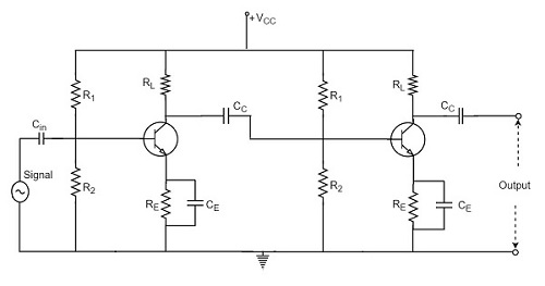
The built-in list of circuits has a "one transistor common-emitter amplifier circuit" which works very nicely, but I would like observe the operation of a two transistor amplifier. I was therefore wondering if anyone had one to share?

The specific question I am looking to answer is what is happening to the voltages at the point between the two transistors, since I was under the impression that the VBE voltage swing has to be quite small to avoid transistor saturation. Does the same apply to the second transistor in the circuit?

By a two transistor circuit I mean two transistor stages coupled via a capacitor, eg.

enter image description here

\$\endgroup\$
13
  • \$\begingroup\$ There are many two transistor amplifier topologies. Do you want one with both transistors configured as common emitter amplifiers? A very common two transistor topology is a differential pair, which takes two inputs and amplifies their difference. \$\endgroup\$ Commented Jan 22 at 6:10
  • \$\begingroup\$ I just came across this video which helped at lot, but a simple capacitor coupled circuit is what I’m looking for (will update question): youtube.com/watch?v=3CVcyyJyWu4 \$\endgroup\$
    – user84299
    Commented Jan 22 at 6:49
  • \$\begingroup\$ @rhody That design cannot be made to work well. The output signal will be grossly distorted. Period. You should study something that may work, rather than not work. Either include local NFB via emitter degeneration in both stages or else include global NFB to both or find another topology. \$\endgroup\$ Commented Jan 22 at 7:20
  • \$\begingroup\$ Start with Falstad's demonstration CE amp. Duplicate and connect input of the second stage to output of the first. Find out why the amplification of the first stage no longer is almost 10. \$\endgroup\$
    – greybeard
    Commented Jan 22 at 8:04
  • \$\begingroup\$ @rhody Read here where I discussed the stage, recently, in detail. You may wish to study this example, which is similar enough but includes the extremely useful global NFB that makes it a good circuit to study. I'm not interested in belaboring a poor stage pairing as you show. If you are stuck on it, have at it. But I would be interested in providing a useful discussion of this latter example if that would help. \$\endgroup\$ Commented Jan 22 at 9:54

1 Answer 1

1
\$\begingroup\$

The specific question I am looking to answer is what is happening to the voltages at the point between the two transistors since I was under the impression that the VBE voltage swing has to be quite small to avoid transistor saturation.

See this simulation made with microcap v12.
The voltage input is "small", 1 mV peak.
You can see that the intermediate voltage is a little "distorted" (quasi 35 mV peak).
However, the output voltage is quite good (harmonic distortion).
And the overal gain is about "1288" or ~ 64 db.

enter image description here

enter image description here

\$\endgroup\$
2
  • \$\begingroup\$ I discuss the stage here and provide detailed reasoning why it's not something I'd consider as a positive teaching model. I would consider it a quality lesson on reasons why to avoid it, though. On the other hand, I think this quite similar arrangement is worth studying as it includes the use of global NFB to fix ills. \$\endgroup\$ Commented Jan 22 at 10:01
  • \$\begingroup\$ The question more about a basic operational understanding of transistor circuits rather than a design question. But I appreciate your input. \$\endgroup\$
    – user84299
    Commented Jan 22 at 17:10