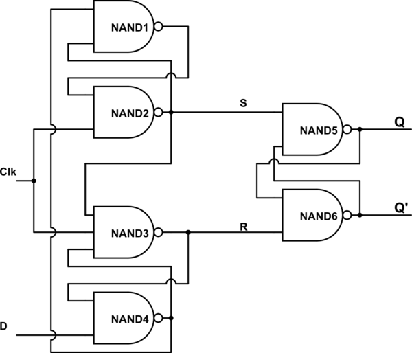
simulate this circuit – Schematic created using CircuitLab
Consider this diagram which represents a positive-edge-triggered D flip-flop. In the analysis of this circuit, my book (Morris Mano) says that when the value of D = 0 and CLK is set to 1, then the value of the Reset variable and Set variable are 0 and 1 respectively.
How can it make such a prediction? Clearly, the output of NAND4 has to be 1 and the lower two inputs of NAND3 have to be 1, but the above input can be either 0 or 1. Also, one input each of NAND 1 and 2 has to be 1. But their outputs can be 0, 1 or 1, 0 respectively. Hence the value of S can be 0 and that of R can be 1. Then why is everyone so sure that R has to be 0 making the output latch always in a reset state?
