0
\$\begingroup\$

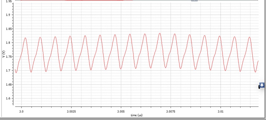
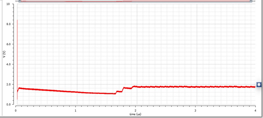
I am designing a low power phase locked loop in cadence with a phase detector, charge pump and VCO.The control voltage output for my circuit at the output of charge pump is as shown below

Control voltage output

But when I zoomed into the waveform I saw some oscillations like this

Control voltage when zoomed

Does this mean that my PLL is not locking properly because I thought, the control voltage must be constant when locked. But, here it is varying for 0.1Vpp. So how should I interpret my result? Is it right or wrong? Please, any help is appreciated.

\$\endgroup\$
5
  • \$\begingroup\$ Is your oscillator frequency anywhere near 1.3GHz by any chance? \$\endgroup\$
    – user16324
    Commented Apr 16, 2017 at 11:46
  • \$\begingroup\$ Yes, the VCO frequency is from 900MHz to 1.33GHz \$\endgroup\$
    – Swap
    Commented Apr 16, 2017 at 11:48
  • \$\begingroup\$ I count about 13 cycles per 10nS. The frequency at the PSD doesn't happen to be around 1.3GHz does it? If so, that's entirely what I would expect for a plain PLL without explicit HF filtering. It would help to post a schematic of what you have. \$\endgroup\$
    – Neil_UK
    Commented Apr 16, 2017 at 11:48
  • \$\begingroup\$ I wanted to post the schematic, but I couldn't. madfeekree.wordpress.com/2010/11/30/… The control voltage from the charge pump is the voltage control to the VCO. So depending on the voltage the frequency of VCO varies from 900MHz to 1.33GHz. What I have shown is the control voltage input itself. \$\endgroup\$
    – Swap
    Commented Apr 16, 2017 at 11:55
  • \$\begingroup\$ Then that waveform is merely the reaction of the charge pump to each cycle of the VCO. Your loop filter will eliminate this signal, unless it has a GHz+ bandwidth. It looks like there are lower frequency components superimposed on it, though, and they may be a bigger concern. \$\endgroup\$
    – user16324
    Commented Apr 16, 2017 at 12:41

2 Answers 2

1
\$\begingroup\$

To properly design a PLL from scratch requires , understanding of Loop transfer functions of each element and closed loop under various conditions.

Lock-up time, Jitter reduction of clock. Phase Margin. bode Plot, lead-lag compensation filter. 2nd, 3rd or 4th order. ( See Analog devices jitter reducing PLL clocks)

Phase detector gain and limitation with frequency error, test methods of measure phase margin and stress conditions: data patterns, SNR, Temp, voltage

There is more but you have successfully detected your phase error as a control voltage ripple from charge pump filter.

The first step should be to define your design goals and specs, then validate.

Then you can decide if it is right or wrong!

I think it can be improved. But you can use V/MHz and integrate V to get phase jitter over the time 8n interval of Vc for vco, but don't stop there.

\$\endgroup\$
0
\$\begingroup\$

Variation in the VCO control voltage will of course cause variation in the VCO frequency.

However, variations at the PSD rate only cause harmonic sidebands, indistinguishable from ordinary harmonic distortion, and we rarely rely on or expect the VCO itself to be harmonic free.

\$\endgroup\$

Your Answer

By clicking “Post Your Answer”, you agree to our terms of service and acknowledge you have read our privacy policy.

Not the answer you're looking for? Browse other questions tagged or ask your own question.