9
\$\begingroup\$

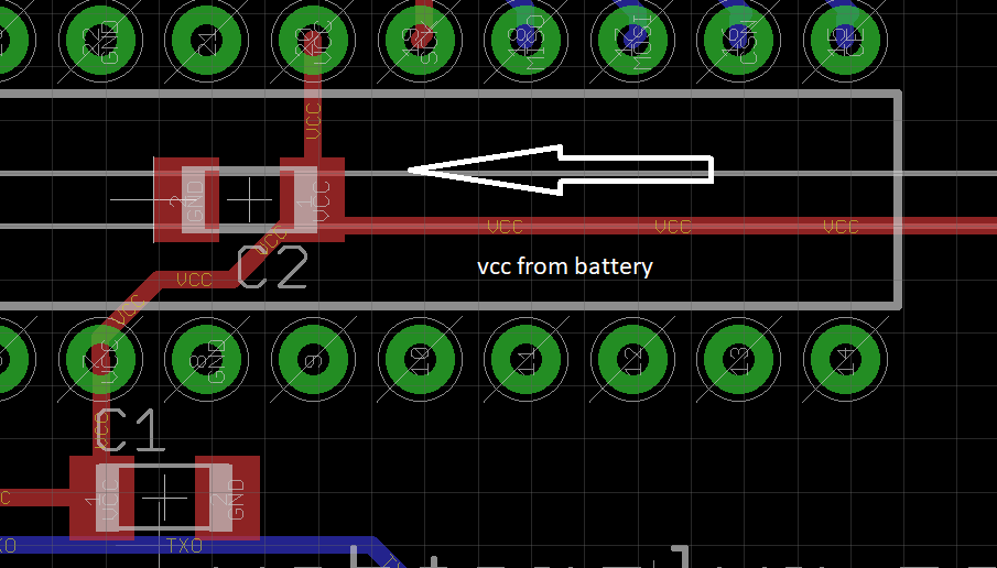
I'm designing a PCB layout with an ATmega328 + NRF24. I know perfectly the need of the decoupling caps, C1 and C2 in my image.

My trouble is following: VCC coming from battery (with a 0.1 µF in parallel).

You note that VCC cross C1 (1206 ceramic 0.1 µF) and goes to pin 20. From C1 VCC goes to pin 7 and from pin 7 on the other decoupler capacitor (C2, again 1206 ceramic 0.1 µF).

Is it right OR I need divide the VCC in two branches, every one "going" to one cap?

Enter image description here

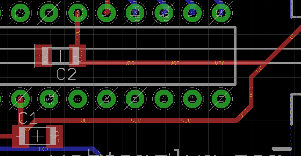
To explain, this is other layout:

Enter image description here

\$\endgroup\$

1 Answer 1

14
\$\begingroup\$

Use the first layout. There is no need to split the Vcc feeds like that.

Other issues:

  1. The ground connection to each cap is also important, in many cases even more important, than the power connection. You haven't show that at all. Getting that right should be your first concern. There should be a short trace directly back to the nearest ground pin without running across the ground plane. Since this is a thru hole part (haven't you heard about the 1990s yet?), the ground pin is a good place for the part to connect to the global ground net or plane.

  2. 100 nF is skimpy. Nowadays, there is little reason to go below 1 µF. 100 nF was the common bypass size back in the Pleistocene because of available technology, not because of being optimum. Today's 1 µF multi-layer ceramic caps are smaller, have less series inductance, and have lower impedance over a wider frequency range than the 100 nF thru hole caps of ancient times.

  3. 1206 package is silly. Why deliberately pick something unusual when the more mainstream 0805 would be at least as good electrically, and cause less space constraints in layout? 0805 is still easy to hand-solder. 0603 is easy too, although handling parts that tiny can be more of a hassle. 0402 can be done by hand, but I'd rather not.

\$\endgroup\$
5
  • 1
    \$\begingroup\$ Thank you for the articulated answer. For 1206, 'cause I did try to solder them and I can do. I cannot do the 0603 (too difficult for me). For the GND plane, I use entire TOP and BOTTOM layer as GND plane, so I can save several links. Thank you another time! \$\endgroup\$
    – sineverba
    Commented Dec 26, 2017 at 14:59
  • 1
    \$\begingroup\$ One more suggestion: consider wider copper power tracks. Also note that C2 is at the top; if you plan placing IC also at the top you will have hard times placing one of the parts. \$\endgroup\$
    – Anonymous
    Commented Dec 26, 2017 at 16:23
  • \$\begingroup\$ @Anonymous track is about 3v and it is 16mil diameter. Do you hint to increase it? C2 is on the top but I will use a socket for atmega, I will not solder direct on pcb... thank you for the advice btw! \$\endgroup\$
    – sineverba
    Commented Dec 26, 2017 at 22:37
  • \$\begingroup\$ It actually depends on the current flowing. It can be as wide as 50 mil (size of the capacitor's pad) if space permits. \$\endgroup\$
    – Anonymous
    Commented Dec 26, 2017 at 22:42
  • \$\begingroup\$ I don't often (at all) post here, but I always enjoy your answers. +1. \$\endgroup\$
    – Liam M
    Commented Dec 27, 2017 at 5:22

Your Answer

By clicking “Post Your Answer”, you agree to our terms of service and acknowledge you have read our privacy policy.

Not the answer you're looking for? Browse other questions tagged or ask your own question.