0
\$\begingroup\$

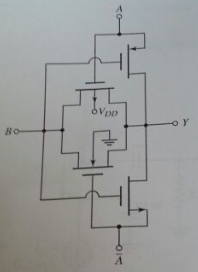
The question is which logic function does this circuit implement if A and B are input and Y is output?

I'm not familiar how 4-terminal MOSFET works but trying to solve Y using A=0 B= 0

The abovest transistor wouldn't be turned on because \$V_{SG} = 0\$

The belowest transistor also cannot be turned on because \$V_{GS}\$ is negative.

For the transistor having \$V_{DD}\$ at base, which side should we choose as a source?

Edit: I still don't know where to expect source when \$V_{DD}\$ and \$GND\$ are ignored as it is said in the comments. I would appreciate an explanation in solving this.

enter image description here

\$\endgroup\$
5
  • \$\begingroup\$ Note the top transistor is N type and the bottom one is P type. So A=0 B = 0, notA = 1 so the bottom transistor is ... ON. And for your second question ... either, Choose whichever is closer to Vdd at the time. \$\endgroup\$
    – user16324
    Commented Jan 12, 2018 at 12:13
  • 1
    \$\begingroup\$ I'm not familiar how 4-terminal MOSFET works The 4th connection is the bulk, substrate or backgate its the piece of silicon the MOSFET is made from. To make the substrate not interfere with anything it is almost always connected to Ground (NMOS) or Vdd (PMOS) and then it's of little use to draw it. It makes no sense that it is drawn here in this circuit, it's not done for the two transistors on the right. This makes the drawing inconsistent and confusing (to beginners). \$\endgroup\$ Commented Jan 12, 2018 at 12:33
  • \$\begingroup\$ For the transistor having Vdd at base That's not the base, it's the bulk as explained above. That transistor is a PMOS, same as upper right. Likewise the transistor with bulk connected to ground is an NMOS like the bottom right one. Just ignore that Vdd and ground connection! Whoever drew this should be ashamed for not being consistent. \$\endgroup\$ Commented Jan 12, 2018 at 12:36
  • \$\begingroup\$ Thanks. An old exam question, the teacher probably aimed to teach different conventions. I would better check old notes because I forgot or didn't learn at all about about this. \$\endgroup\$
    – user175079
    Commented Jan 12, 2018 at 12:43
  • \$\begingroup\$ @user175079: Note: the bottom two MOSFETs are both N-channel, the top two are both P-channel; (as Bimpelrekkie said) using two different symbol conventions. This doesn't make much sense other than to confuse the reader. \$\endgroup\$
    – Curd
    Commented Jan 12, 2018 at 14:14

2 Answers 2

1
\$\begingroup\$

The 4 terminal MOSFET is a symmetrical device. Drain and source are interchangeable. For a 3-terminal MOSFET the source is the one that's connected to the body.

What you have here is called a transmission gate. Notice that the top MOSFET is a PMOS while the bottom is an NMOS, so they will both be 'on' at the same time (when \$\bar{A}\$).

\$\endgroup\$
0
\$\begingroup\$

I believe this would be an XOR gate.

The top transistor is only on if AB is 10 (p type with A high and B low) The 2nd to the top transistor is only on if AB is 01 (p type with B high and A low) The 2nd to bottom is only on if AB is 00 (n type with A! high and B low) The bottom is only on if AB is 11 (n type with B high and A! low)

So the truth table is:

A B | Y

0 0 | B = 0

0 1 | B = 1

1 0 | A = 1

1 1 | A!= 0

\$\endgroup\$

Your Answer

By clicking “Post Your Answer”, you agree to our terms of service and acknowledge you have read our privacy policy.

Not the answer you're looking for? Browse other questions tagged or ask your own question.