3
\$\begingroup\$

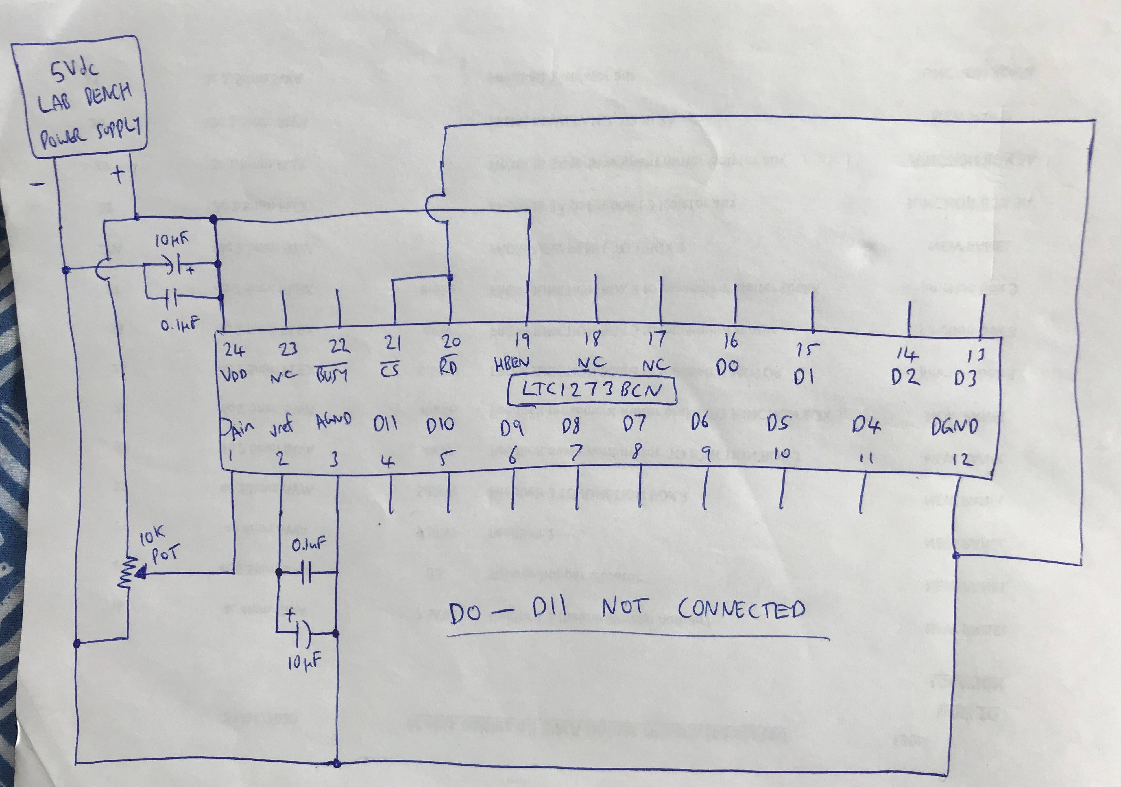
I am connecting a 10k potentiometer to an ADC chip (LTC1273BCN) that has a 12-bit parallel output, like in the diagram at the end of the post. The 12-bits will be connected to an FPGA input bus after I can get it to work correctly. The ADC chip circuit is powered off a stable 5V from a lab benchtop power supply.

I have tied the CS and RD inputs low as I thought this will continuously run the conversion but maybe this is my problem, I am unsure.

When I measure the voltage of the 12 output pins, only pin 14 (D2) seems to be high, the rest are 0V. The Ain voltage is perfect between 0 and 4.99V from the potentiometer, and I have tied the HBEN input to 5V as I want to use all 12-bits in one conversion.

Any advice as to how to use this chip correctly? Will I have to pulse the CS and RD inputs low to get the chip to behave as I would like? I don't really want to use signals from the FPGA to control the analog to digital conversion.

EDIT

Below is my reasoning behind the pin connections:

Pin 1 : 0V to 5V from potentiometer, to be converted to 0 to 4095 by ADC chip.

Pin 2 : I haven't used this pin but have attached capacitors to pin 3 according to datasheet.

Pin 3 : Tied to analog ground which is the same ground as chip supply.

Pins 4 to 11 : D11 to D4 output bits are left unconnected.

Pin 12 : Tied to ground of power supply.

Pins 13 to 16 : D3 to D0 output bits are left unconnected.

Pins 17 and 18 : Left unconnected as in datasheet.

Pin 19 : Tied to 5V to use the full 12 bits in one conversion instead of splitting into 2 conversions in one byte.

Pin 20 : Tied to ground for continuous conversion ( if this is possible).

Pin 21 : Tied to ground to allow for continuous conversion ( if this is possible).

Pin 22 : Left unconnected as I am not using it.

Pin 23 : NC

Pin 24 : +5V from power supply to power up ADC chip.

Thanks everyone.

ADC Circuit diagram image

\$\endgroup\$
5
  • \$\begingroup\$ Please provide a data sheet link and explain what it is in the DS that prompted you to choose the above circuit to trial. \$\endgroup\$
    – Andy aka
    Commented Mar 27, 2021 at 11:04
  • \$\begingroup\$ @Andyaka Have just added datasheet and will edit the question now. \$\endgroup\$
    – David777
    Commented Mar 27, 2021 at 11:05
  • 1
    \$\begingroup\$ From what I can see in the datasheet, you can't continuously pull RD and CS low. There needs to be a delay between conversions and between two read operations (t10 and t11 from the datasheet). \$\endgroup\$
    – StarCat
    Commented Mar 27, 2021 at 11:10
  • 1
    \$\begingroup\$ How are you expecting the FPGA to know when the data is valid so that it can read it reliably? \$\endgroup\$ Commented Mar 27, 2021 at 22:10
  • \$\begingroup\$ @DavidSchwartz Yeah, I have learned from this post that I have a design flaw. I am going to now use the FPGA to start the conversion by pulling the pin low, and then after the conversion time, set the pin high again and read/store the ADC value into a register. Then repeat this process synchronously after a time delay. \$\endgroup\$
    – David777
    Commented Mar 27, 2021 at 22:15

3 Answers 3

6
\$\begingroup\$

Justme gave the answer, you have to clock it.

continuous conversion without having to initialise and command the conversion?

That would mean the ADC would change the level of its output pins every time it does a new conversion. Counting uneven propagation delays, skew, etc, if the device that reads these pins reads them at the wrong time, it will get some bits from the previous value, some bits from the new value, and some bits in transition which will be garbage.

That's why synchronous logic uses clock to synchronize things and ensure signals are sampled when they are valid.

If an ADC does continuous conversion, it must have an output with an edge to indicate when the data is valid and can be sampled by the next device. You will need to apply proper clock domain crossing to that in your FPGA. It is simpler to just generate the timing signal from the FPGA, plus you will get a stable sample frequency instead of whatever RC internal oscillator the ADC uses.

Note for 300ksps you don't need a flash ADC, a SAR will do just fine, and it's cheaper.

EDIT:

Mainly because I have to use opto-couplers between the FPGA and the ADC bits, so I will have to also isolate the CS and RD signals from the FPGA too.

OK, so you want an isolated reading on a potentiometer. I really wonder why, but there are much simpler solutions for that.

  • SPI ADC. Pretty cheap, less opto couplers. It will be fast enough.

  • Isolated ADC (check mouser/digikey). Should be expensive.

  • Cheap micro as the ADC, output the data on a UART, isolate that, and instantiate a UART receiver in your FPGA.

  • Or turn the pot signal into PWM, or variable frequency, or pulse density modulation (many ways of doing this, 555, opamps, etc), isolate it with one opto, and read the duty cycle, period, etc with a timer/counter in your FPGA.

\$\endgroup\$
11
  • \$\begingroup\$ I would like isolated signals between the FPGA and the potentiometer circuit as the FPGA development board is powered through the computer's USB port and the potentiometer circuit is supplied from a 5V power supply. So they need to be isolated. \$\endgroup\$
    – David777
    Commented Mar 27, 2021 at 20:11
  • \$\begingroup\$ It's not dangerous voltage, you could power the pot from the FPGA board instead. \$\endgroup\$
    – bobflux
    Commented Mar 27, 2021 at 21:34
  • \$\begingroup\$ The only problem with doing that is, there is nowhere on the FPGA board to get 5V. Everything is 3.3V \$\endgroup\$
    – David777
    Commented Mar 27, 2021 at 21:45
  • \$\begingroup\$ You can use 3V3 to power a pot, it doesn't care about voltage... \$\endgroup\$
    – bobflux
    Commented Mar 27, 2021 at 23:00
  • \$\begingroup\$ @David777 You can disable USB powering and use an external power supply on every development board I've ever seen (and in 25 years in industry I've seen a few!). \$\endgroup\$
    – Graham
    Commented Mar 28, 2021 at 8:28
5
\$\begingroup\$

No it won't work like that, page 15 of the datasheet describes how the chip bus works.

At least some of the control signals need to have transitions, this chip is intended to be sitting on a memory bus so it looks like RAM or ROM chip.

\$\endgroup\$
9
  • \$\begingroup\$ Ok, I see. My next question is do such ADC chips exist that allow for continuous conversion without having to initialise and command the conversion? \$\endgroup\$
    – David777
    Commented Mar 27, 2021 at 11:19
  • 1
    \$\begingroup\$ Most likely such chips exist, I am quite sure of that. \$\endgroup\$
    – Justme
    Commented Mar 27, 2021 at 11:21
  • \$\begingroup\$ Ok, I will see what I can find, thanks. \$\endgroup\$
    – David777
    Commented Mar 27, 2021 at 11:24
  • \$\begingroup\$ Maybe my best solution is to use the FPGA to control the ADC conversion or another external circuit like a 555 timer to generate the signals? \$\endgroup\$
    – David777
    Commented Mar 27, 2021 at 11:34
  • \$\begingroup\$ Maybe. Hard to say as you don't mention what are you doing as a whole. I do hope you are not seriously thinking of adding extra hardware, especially a 555 timer, to help interfacing something to an FPGA which already is reconfigurable hardware. \$\endgroup\$
    – Justme
    Commented Mar 27, 2021 at 11:41
4
\$\begingroup\$

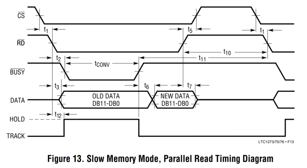
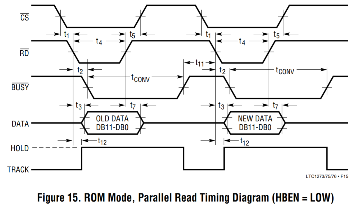
Holding CS and RD low permanently will force the ADC to make one single conversion right after power is applied. That value will be presented to the output bus until you remove power. No further conversions will be performed: -

enter image description here

enter image description here

\$\endgroup\$
4
  • \$\begingroup\$ Ok, I see. My next question is do such ADC chips exist that allow for continuous conversion without having to initialise and command the conversion? \$\endgroup\$
    – David777
    Commented Mar 27, 2021 at 11:19
  • \$\begingroup\$ @David777 try looking for a flash conversion ADC \$\endgroup\$
    – Andy aka
    Commented Mar 27, 2021 at 11:39
  • \$\begingroup\$ Do flash converter ICs for 12 bit exist? \$\endgroup\$
    – David777
    Commented Mar 27, 2021 at 12:11
  • 1
    \$\begingroup\$ I don't know. I expect 8 bit ones work but, if you are looking for a real solution to try out look for a converter that can be set to run continuously or toggle the CS and RD lines with an oscillator. \$\endgroup\$
    – Andy aka
    Commented Mar 27, 2021 at 12:28

Your Answer

By clicking “Post Your Answer”, you agree to our terms of service and acknowledge you have read our privacy policy.

Not the answer you're looking for? Browse other questions tagged or ask your own question.