What we need to understand circuits
Where is Vin supposed to go?
A question that may appear trivial at first glance, but it actually conceals a deep philosophical underpinning – the philosophy of latches and flip-flops. This underlying philosophy is essential for comprehending specific circuit designs such as the one we are examining. However, it is a subject that is often overlooked or inadequately covered in traditional textbooks.
How to develop a philosophy for understanding circuits
The answer is simple – with a lot of thinking, comparing, and contrasting, we seek the common idea in specific circuit solutions. However, this requires thinking... a lot of thinking... For comparison, I have been pondering this problem since the 70s when I was a student, while you have been doing it for a week. But I will save you those 50 years by telling you this story. Here I will trace the idea behind this original circuit solution by using a six-step CircuitLab scenario. For simplicity, I have used DC simulations, but they do not fully represent circuit operation. Maybe in the future I will also add time-domain simulations.
How to make the simplest non-inverting latch
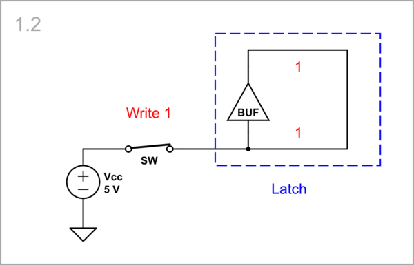
The recipe is extremely simple and intuitive - we connect the output of a non-inverting amplifier (a 1-input logic gate or buffer BUF) to its input. Thus, we force it, with the help of "self-reinforcing positive feedback" to maintain (remember) its output voltage in one of two possible values - 0 V (logic 0) or 5 V (logic 1).

simulate this circuit – Schematic created using CircuitLab
How to control the simplest latch
Now, we need some way to toggle this most basic memory cell (switch between its two states). This is typically done by applying a voltage to the input. But what is the input here, since the output and input are connected? They are one and the same. Obviously, with this "brute force" method of control, a conflict can arise between two voltage sources, the input voltage source and the buffer's output, when they have different voltages. Interestingly, however, this method is widely used in SRAM memories.
Vin = 5 V: For example, to switch the circuit to the "1" state, we can apply 5 V through an SW switch. But at the same time, its output may be in the "0" state, and then a "short circuit" will occur. Fortunately, however, the circuit will switch instantaneously to the "1" state and the "short" will disappear. The input source only needs to be "stronger" than the buffer's output to overpower it.

simulate this circuit
Vin is disconnected: Once we have switched the latch to "1", we need to leave it alone to remember the data stored in it. To do this, we need to remove the input source because it would keep the latch constantly in the "1" state and we would not be able to change its state to "0" by another input signal.

simulate this circuit
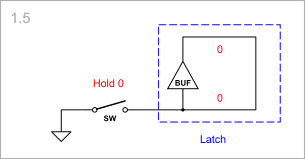
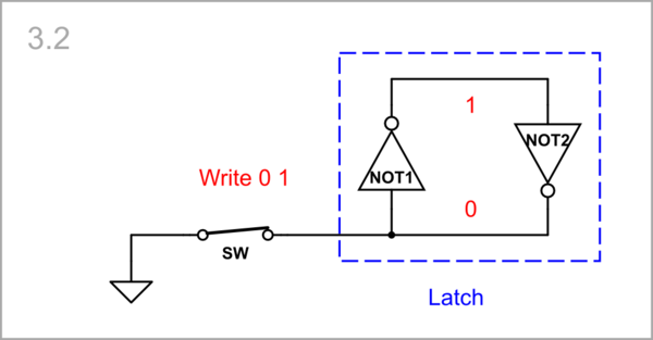
Vin = 0 V: Conversely, to set the circuit to "0", we apply 0 V. The output can be already at "1", and that is again "short circuit". But the circuit will quickly switch to "0", and the "short" will disappear.

simulate this circuit
Vin is disconnected: As above, once we have switched the latch to "0", we need to leave it alone to remember the data stored in it. Again, we remove the input source because it would keep the latch constantly in the "0" state and we would not be able to change its state back to "1".

simulate this circuit
Implementation
By two SPST switches: So, our simplest latch has a total of three states - two short ones where it is connected to the input source, and one long one where it is disconnected from the input source. We can implement it with two SMPT switches, one of which is connected to 5 V and the other to 0 V (or with one switch with neutral middle position).
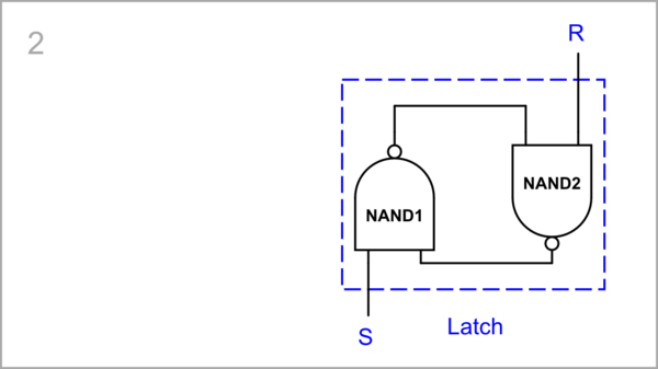
By two cascaded NOT gates: But, as you have noticed, this is not the generally accepted way to control a device using a continuously connected input voltage source with two values. To solve this problem, they were forced to connect (cascade) two 2-input NAND gates in a loop and control this RS flip-flop with two separate input sources. Like the previous circuit, this one also has three states - a short "0" on one (S) or the other (R) input for switching to the corresponding state, and two "1"s for disconnecting the circuit from the input sources.

simulate this circuit
Am I missing something, or what is the point in using NAND gates at all, won't they just function as NOT gates if both inputs are high or low at the same time?
In the classic RS flip-flop, the two inputs of the NANDs must be separate because this allows for "unidirectional" (only with "0") control. When they are in "1", the inputs are "off" (they do not affect the circuit).
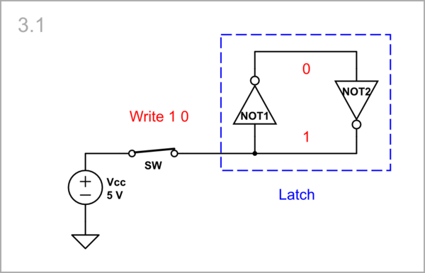
In your circuit, simple 1-input NOT gates must be used to control it with only one input voltage source (see the explanations below).
How to make a T flip-flop
Of course, a more obvious reason to make flip-flops using NOT gates is that they are more common and technological. But in your case, there is a much more valid reason for this. Let's see what it is like.
The problem
The task is to alternately toggle a latch by pressing a simple SPST button, i.e., to make something like a T flip-flop.
Basic idea
We can borrow the trick by which a D flip-flop is made into a T flip-flop - at the input of the D flip-flop, the inverse value of the current input voltage should be waiting. So the question comes down to having that inverse value.
Implementation
Vin = 5 V: So if the button outputs 5 V, the next (inverse) value should be 0 V.

simulate this circuit
Vin = 0 V: And accordingly, if the button outputs 0 V, the next (inverse) value should be 5 V.

simulate this circuit
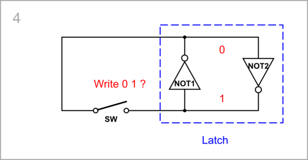
Vin = Vout: Aha, that is why we need NOT gates - because we can take the inverse of the input voltage from the output of the first NOT1 gate! So we simply connect the switch between the forward and inverse terminals of the latch.

simulate this circuit
Adding a capacitor memory
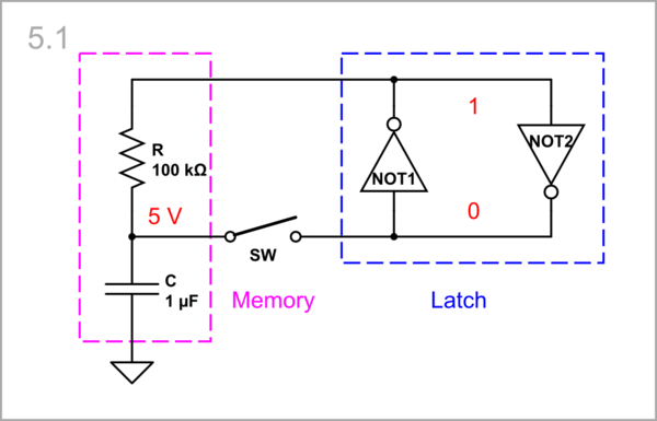
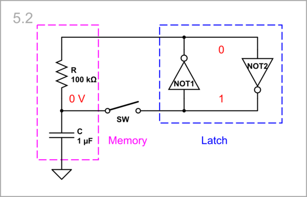
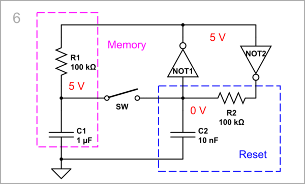
But a new problem arises - when the button supplies the reverse voltage from the output of NOT1 to its input, it instantly starts to change in the opposite direction and the gate will not be able to switch at all. Then let's temporarily store the NOT1 output voltage across a capacitor C.
Now, when the reverse value is "1", the capacitor is charged to 5 V. When we push the SW button, a logic "1" is applied to the latch.

simulate this circuit
Conversely, when the reverse value is "0", the capacitor is charged to 0 V. When we push the SW button, a logic "0" is applied to the latch.

simulate this circuit
Just maybe the time between two button presses should not be too short for the capacitor C to recharge.
About the NAND inputs
Should the inputs on both NAND gates really be connected respectively together?
Yes, in your "T flip-flop" , the two inputs of the NANDs (especially NOT1) must be joined because this allows for "bidirectional" (both with "0" and "1") control.
Adding a capacitor reset circuit
A problem is that this "push-button T flip-flop" has an undetermined initial state. We can solve it by connecting another but smaller RC integrating circuit to the input of NOT1. It outputs a short "0" when the power is turned on.

simulate this circuit
Summary
The simplest memory cell (latch) can be made by connecting a logic buffer's output to its input. The self-reinforcing positive feedback holds it in one of its two possible states 0 V (logic 0) or 5 V (logic 1).
The simplest way (that is widely used in SRAMs) to toggle this memory cell between 0 and 1 is by briefly applying 0 V or 5 V to its common input/output. This can be made by a push-button (as in your circuit) or a pass-transistor as in SRAMs.
With this crude control method, a conflict can occur between the input voltage source and the buffer output if they have different voltages; so, the input source must be more robust than the buffer output to effectively override it.
After it has done its job, the input source can be removed because the cell continues to remember.
Thus, a latch requires a third, "idle" state where the input source is isolated from the common input/output pin.
In your specific "man-controlled circuit" , this idle state is achieved by releasing the push-button. Today we would call this a "high-impedance state" (i.e., the button adds another high-impedance state to the existing 0 and 1 states).
In classic flip-flop circuits, the disconnecting of the input source is achieved by adding another 2-d input to the logic gate (using a 2-input NAND). Now, only the zero level is active; the 5 V level is inactive.
This requires adding another logic gate (another 2-input NAND) after the first one so that the latch can be toggled back by its second input. The result is the classical configuration of two cascaded NANDs in a loop (often drawn as two cross-coupled logic gates).
Your T flipflop configuration needs the NAND's inverted output for another reason - to change alternately its state. But it does not need 2-input NANDs; so it can be implemented by 1-input NOT gates.
The NAND1's inverted output is used as a next input signal. It is temporarily stored in a C1 capacitor memory.
The circuit is initially set by another smaller R2C2 integrating circuit.


