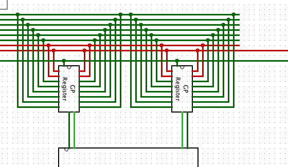
Joe Hass covers the traditional way, replacing the AND gates with tristate logic. This is the way things were done with TTL chips in the 1970s and it is still quite common at the PCB level.
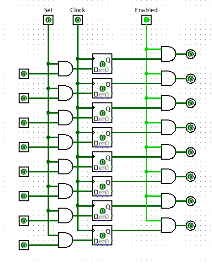
However inside an FPGA, tri-state buffers are no longer supported (except at the external pins) since about the start of this century. (ASICs differ in this respect; thanks to Joe Hass for the correction) The synthesis tool may accept a circuit description based on tri-states, but implement it by transforming the circuit into something entirely different ... usually the first stage is a row of AND gates connected to the Enable as in your example.
If your register genuinely has AND gates on the enable line, then it is a more recent design, and you need an extra stage of logic to create the bus.
That stage is simply an OR gate on each bus bit with N inputs, one input for each source (GP register etc) driving the bus. The outputs from each source are simply ORed together, and the OR gate output drives the bus. The N-input OR gate can be implemented in several ways - e.g. as a tree of 2-input OR gates if that's what your logic system offers.
This works because if one Enable is high, all other sources are driving 0 on the bus.
It is more reliable than the tri-state approach because if several Enables are high, the result is meaningless nonsense (several outputs ORed together) instead of a short circuit across the power supply (where one source is '0' and the other is '1'), possibly causing a small fire...
Both approaches work : but if you are designing logic inside an FPGA or ASIC, this one is strongly preferred.
(An alternative way of eliminating tri-states is based on an N:1 multiplexer. If you draw out the usual implementation of a 2:1 multiplexer you will find the two approaches are essentially the same).


