8
\$\begingroup\$

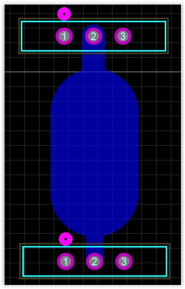
I am designing a PCB, and 10 A-15 A current is flowing in a trace. I think a 300 thou track should be used for 1 oz Cu-thickness. I see that it is impossible to connect two pads with a 300 thou track, because it violates design rules and also other pads are included into the trace, which is undesired.

Enter image description here

Figure: 300 thou width trace connection, between pad and the 300 thou trace there is a 80 thou trace (above) and a 60 thou trace (below).

What I ask is:

Can this connection carry the current that a 300 thou trace can carry? Which measurements must be taken?

\$\endgroup\$
3
  • 2
    \$\begingroup\$ Unles you Need pins 1 and 3, I'd suggest you get rid of them - or change the design so each carries the same signal as pin 2. I'd also suggest a "flood fill" of the area. Lastly, consider just using the PCB to hold some heavy duty posts, and run wire between the posts. At least 18AWG: see powerstream.com/Wire_Size.htm \$\endgroup\$ Commented Nov 22, 2014 at 10:58
  • 2
    \$\begingroup\$ @Alan Campbell This 3 pin device is a mosfet, and all pins are necassary, maybe I should consider seperating the legs of transistor with distance 2 inches instead of 1 inch (standard). \$\endgroup\$
    – electro103
    Commented Nov 22, 2014 at 22:08
  • 1
    \$\begingroup\$ In that case, as other have answered: it's all about how hot the track will get. Scorched PCBs smell awful. Running 18AWG (or 16) on your power and return lines should do the trick. \$\endgroup\$ Commented Nov 24, 2014 at 7:08

3 Answers 3

16
\$\begingroup\$

There are two values you need to worry about: voltage drop, and power dissipation. Both are simple Ohm's Law and are functions of the trace resistance.

The trace resistance is a product of its cross sectional area, and its length.

Reduce the length and you reduce the resistance. Reduce the width and you increase the resistance.

So you can have a shorter run of a narrower trace and still handle the current.

The formula for calculating the resistance of a trace is:

$$ R = \rho \frac{l}{A} \cdot (1 + (\alpha \cdot \Delta T)) $$

  • \$\rho\$ is the resistivity, which for copper is \$1.68×10^{-8} \Omega/m\$.
  • A is the cross-sectional area in m²
  • l is the trace length in m
  • \$\alpha\$ is the temperature coefficient, which for copper is 0.003862 at 20°C.
  • \$\Delta T\$ is the temperature difference from 20°C

So for a 300 thou (7.62mm) trace at 1oz, which is a thickness of 0.0347mm, a rectangular cross-section would be

$$ 0.00762 \times 0.0000347 = 0.000000264m² $$

Of course, with etching and other factors it won't be as thick, nor perfectly rectangular, so reduce that a little - let's say for the sake of convenience it's 0.0000002m².

Then you have a trace that's 0.05m long (5cm). What is the resistance of that trace at, say 23°C?

$$ R = 1.68×10^{-8}\frac{0.05}{0.0000002} \cdot (1 + (0.003862 \times 3)) $$ $$ R = 1.68×10^{-8} \times 250000 \times 1.011586 $$ $$ R = 0.00425\Omega $$

So once you have the resistance, and you know the current, you can apply simple Ohm's Law to it. Say 15A, your upper value.

The voltage dropped across that trace is $$ V=IR = 15 \times 0.00425 = 0.064V $$

The power dissipation will be $$ P=I^2R = 15 \times 15 \times 0.00425 = 0.956W $$

So now you can calculate what the voltage drop and power dissipation would be over your small traces to see if it's tolerable.

There are also various tricks you can employ for handling larger currents. One of the most common (and old-school) is to leave the traces unmasked, then flood them with extra solder. This massively increases the cross-sectional area thus reducing the resistance. You can also use electro-plating to achieve a similar result, though this is considerably harder to do, especially in just a small area of the board.

Using wires instead of (or as well as) traces can also be done.

As an aside, you should also consider if the connections, and the pins used in your connectors, are suitable for carrying up to 15A.
\$\endgroup\$
2
  • \$\begingroup\$ Even narrower trace like 10thou can carry 15 Amperes? There are some online tools that calculates the pcb trace width, like circuitcalculator.com/wordpress/2006/01/31/… \$\endgroup\$
    – electro103
    Commented Nov 22, 2014 at 10:02
  • 8
    \$\begingroup\$ It's not a question of "can it take the current", but a question of "will the voltage across that trace drop more than I would like, and will it heat up more than I can tolerate?". \$\endgroup\$
    – Majenko
    Commented Nov 22, 2014 at 10:39
3
\$\begingroup\$

In the end its all about power dissipation resulting in heat. Wider traces obviously reduce resistance, improve heat dissipation and thus are optimal. Realize that while trace resistance is a function of width and length, heat dissipation also is. A trace twice as long may have double the trace resistance but it also can dissipate about twice as much heat. Therefore, you mainly have to care about how much temperature increase you can tolerate.

-> Twice the trace length means more heat overall, but not more heat per trace length unit.

So calculate how much temperature increase you can afford and just keep the length of the thin traces as short as possible. There is no absolute minimum per se.

\$\endgroup\$
1
  • 1
    \$\begingroup\$ I think the two parts of the heat issue is heat generated by the resistance itself, and the ability for the trace to sink heat (it's thermal resistance) which can also be heat generated from other areas of the PCB. A 'fat' trace will inherently generate less heat, because it has less resistance so the current can flow with less losses. \$\endgroup\$
    – KyranF
    Commented Nov 22, 2014 at 12:44
-3
\$\begingroup\$

Just as the strength of a chain is only strong as it's weakest link, the current carrying capability of a trace is only as good as its thinnest section. For the sample you provide, it is the 60 thou section. Although the "extra" copper provided by the thicker section helps with heat removal, it does nothing for the current carrying capacity of the trace. So, the number you should use for the calculations, should be 60 not 300 thou. If the 300 thou trace is good for 15A, then the sample trace would be good only for 15A x (60/300) = 3A.

\$\endgroup\$
2
  • \$\begingroup\$ -1 for a bunch of reasons, but "the current carrying capability of a trace is only as good as its thinnest section" is not true. This view is too simplistic for the real world of high current PCB design. \$\endgroup\$
    – Matt Young
    Commented Nov 29, 2014 at 5:32
  • \$\begingroup\$ @Matt Young I would agree that I am giving a simple answer. But simple does not mean it is not true. If you look at the equations involved (I = E/R, R = k/A, A = h x w) you obtain I = Kw/h. Which shows that the current capability of the trace is directly proportional to the width of the trace! \$\endgroup\$
    – Guill
    Commented Nov 29, 2014 at 7:11

Your Answer

By clicking “Post Your Answer”, you agree to our terms of service and acknowledge you have read our privacy policy.

Not the answer you're looking for? Browse other questions tagged or ask your own question.