1
\$\begingroup\$

[POST IS EDITED]

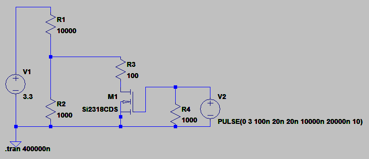
I'm trying to debug a circuit shown in Fig. 1.

enter image description here

The gate of the FET is driven with a square wave 0...3 volts. The voltage source V1 = 3.3V. The circuit is built to control the voltage presented to the non-inverting input of an operational amplifier. R2 and R3 are trimmers, so the two input voltages can be trimmed to different values if needed.

Driving the FET with a square wave I notice a rather odd behaviour. The voltage between R1 and R2 are shown in Fig. 2 as a function of time (green). The voltage of Vgs is drawn blue. enter image description here

As can be seen, the voltage v+ first dips to a negative value and then rises slowly to the steady state value. When the voltage v+ should drop to the lower value (vgs = 3 V) it first overshoots after going down to the steady state. The simulation and oscilloscope measurements agree together.

What could be causing this, and how can i get the voltage between R1 and R2 (green waveform) to be as closes as a square wave as possible. Fet in use is Si2318CDS. Datasheet provided in the comment. I have tried higher Vgs amplitudes han 3V.

\$\endgroup\$
5
  • \$\begingroup\$ Could add more links to the opening post. The FET in use is mouser.com/ds/2/427/si2318cd-244540.pdf \$\endgroup\$
    – user94729
    Commented Dec 17, 2015 at 12:24
  • \$\begingroup\$ Do you have actual oscilloscope images where times and voltages can be seen? \$\endgroup\$
    – PlasmaHH
    Commented Dec 17, 2015 at 12:40
  • \$\begingroup\$ If you are using LTSpice then show a picture of the transient response rather than you hand-drawn effort. \$\endgroup\$
    – Andy aka
    Commented Dec 17, 2015 at 12:45
  • \$\begingroup\$ I am still a rookie regarding MOSFETS, but you might be interested in the Miller plateau or Miller effect. This has something to do with the current that is pumped into the input capacitor of the mosfet. \$\endgroup\$
    – Weaverworm
    Commented Dec 17, 2015 at 12:55
  • \$\begingroup\$ EDIT: waveforms provided from LTSpice. PlasmaHH: oscilloscope measurements agree with the simulated values. \$\endgroup\$
    – user94729
    Commented Dec 18, 2015 at 6:47

2 Answers 2

3
\$\begingroup\$

There is capacitance from the gate to the drain. Normally (as in a power switch) this is more of a concern for the gate drive (especially when the drain voltage is changing a lot and fighting the gate drive), but the capacitance also couples changes in the gate voltage to the drain.

In this case you have 270mV on the drain when it is off, and ~0mV when it is on and the gate drive is more than 10x higher (3V).

There are a variety of techniques to reduce this- a smaller MOSFET will help because it has less capacitance, but you will pay in terms of Rds(on). Another approach is to balance off the injected charge by another transistor driven with something like the opposite waveform. You can find multiple patents describing these techniques.

Good commercial analog switches can have charge injection in the 1pJ range, which sounds low, but it's actually still a problem in some cases.

Edit: From your waveforms you can see two time constants. From the MOSFET datasheet, page 3, "Capacitance" shows the output and reverse transfer capacitances vs. Vds. They increase sharply for low (or, by extrapolation) slightly negative Vds. For large negative Vds the body diode will start to conduct significantly so these waveforms will not scale- if you increase the drive voltage to 10V you will see a change in the shape.

You might want to look at this answer from Andy and (upvote if it is helpful, of course).

\$\endgroup\$
6
  • \$\begingroup\$ Thanks for the answer! The gate of the FET is driven with a function generator, and when the Vgs is measured using an oscilloscope, the rise and fall times are quick - it does not indicate that there is any great capacitive leakage does it? Also, what is the mechanics behind a negative voltage appearing in the node of the non inverting input. \$\endgroup\$
    – user94729
    Commented Dec 18, 2015 at 5:12
  • \$\begingroup\$ I have also edited my question, it now includes more illustrative waveforms. \$\endgroup\$
    – user94729
    Commented Dec 18, 2015 at 6:48
  • \$\begingroup\$ Thanks for the edited answer! I have tried different MOSFETs in LTSpice and nothing seems to work. Is the voltage select scheme of figure 1 even achievable with this kind of an architechture? \$\endgroup\$
    – user94729
    Commented Dec 18, 2015 at 10:01
  • \$\begingroup\$ As I have no idea what you are trying to do, it's difficult to say. \$\endgroup\$ Commented Dec 18, 2015 at 11:10
  • \$\begingroup\$ Well basically i want to control the non-inverting input of an operational amplifier between two states. I have a comparator, which will output either 0V or 3.3 V (upper voltage can be brought higher). The FET of the original circuit was supposed to be driven with the comparator output. \$\endgroup\$
    – user94729
    Commented Dec 18, 2015 at 11:19
0
\$\begingroup\$

This is the drain-gate capacitance. It's a simple R-C circuit coupling the gate voltage (square wave) into the drain circuit.

Considering the impedances, use the smallest (lowest C) MOSFET you can find. (There's a reason small signal JFETs are often used for switching low level signals)

A more detailed analysis needs the MOSFET datasheet and the time axis scale factor (or frequency of the square wave).

\$\endgroup\$

Your Answer

By clicking “Post Your Answer”, you agree to our terms of service and acknowledge you have read our privacy policy.