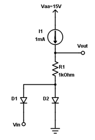
Firstly consider the DC operating point of the circuit.
Vout is the sum of the voltage drop over the 1k resistor and the voltage drop over the silicon diode = 1k * 1mA + 0.53V = 1.53V. (The voltage drop over a silicon diode will be ~0.53V at 1mA).
Now consider the effect of Vin. Diode D2 places an upper limit on Vout (1.53V) and an upper limit of 0.53V on the node where the diodes connect. Using a mathematically idealized model for the diode, it holds that if Vin > 0, the voltage drop over D1 cannot be 0.53V, and D1 will be reversed biased, i.e. Vin has no effect.
However, if Vin < 0, D1 will be forward biased and will pull down the voltage at Vout, Vout = Vin + 1.53V. D2 will be reversed biased and will have no effect.
So the maximum value for Vout = 1.53V and the minimum = -8.47V.
Using the idealized model for the diode we have a half-wave rectified sine with a -10V peak and a 1.53V offset. The average for a half-wave rectified sine is Vpeak/pi, so in this case -10/pi + 1.53 = -1.65 V

