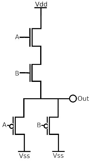
So I know that a CMOS AND gate is made with 2 parallel p-type transistors and 2 serial n-type transistors and an inverter on the output. But can we just make the AND gate similar to the NOR gate -instead to just use 2 serial n-type with 2 parallel p type. The truth table makes up an AND as far as I can see.

-
\$\begingroup\$ Ask yourself: Is this design regenerative? If the input voltages are near the minimum logic high level (for example) will the output voltage still be a valid logic high (or even better, well above the input voltages)? \$\endgroup\$– The PhotonCommented Mar 29, 2018 at 16:06
-
\$\begingroup\$ Are you essentially asking what happens if you swap the nMOS with the pMOS devices and vice versa where the nMOS is the pulldown and pMOS is the pullup? If so then... yeah... the circuit won't behave the same way... \$\endgroup\$– user103380Commented Mar 29, 2018 at 16:07
-
\$\begingroup\$ @KingDuken, I think they're trying to get a minimalist AND gate rather than a NAND + inverter. \$\endgroup\$– The PhotonCommented Mar 29, 2018 at 16:09
-
\$\begingroup\$ Why the p-type has to be in parallel and not in serial? \$\endgroup\$– Miquel VivesCommented Sep 26, 2018 at 18:20
1 Answer
The logic is correct, that does implement the AND function. However, the output impedance is dependent on the input state (sinks more current when inputs are F,F than when they are T, F). This results in odd behaviors that made timings uncertain, and modern CMOS (CD4000B series) gates are almost all two-stage (with a buffer inverter added) gates.
That reasoning does not apply to one-input (inverter) circuits, and a few of those (CD4049UB) are still available, but the two-stage gates have superior gain, so the general run of off-the-shelf CMOS is all buffered. Internal to a complex device, the unbuffered variants are still useful subcircuits.
