1
\$\begingroup\$

I understand that decoupling capacitors are small capacitors (often 100nF) used on VCC/VDD on ICs. When are they most required and when is it just silly using them on every IC.

  • Are they better used at higher operating frequencies?
  • Are they better used with repetitive signals?
  • Are they better used with more important parts of a circuit?
  • Should they always be used on every IC?
\$\endgroup\$
5
  • 1
    \$\begingroup\$ I use them not only one every IC but on every supply pin on every IC. \$\endgroup\$
    – Oldfart
    Commented Jan 7, 2019 at 20:32
  • 1
    \$\begingroup\$ Yes, use one on every supply pin of every IC. Doesn't matter what kind of IC it is or how it is used. \$\endgroup\$
    – CrossRoads
    Commented Jan 7, 2019 at 20:36
  • 1
    \$\begingroup\$ Well, the value would depend on the operating conditions and the IC vendor recommendations. \$\endgroup\$
    – Eugene Sh.
    Commented Jan 7, 2019 at 20:40
  • 1
    \$\begingroup\$ Every power pin of every IC. And if you're doing a transistor-based circuit design, then at every stage of the circuit (judiciously, because your "stage" may be different than mine). \$\endgroup\$
    – TimWescott
    Commented Jan 7, 2019 at 21:02
  • 1
    \$\begingroup\$ I use one on every power pin if possible and a bulk bypass for every few (perhaps 10). I say if possible because if I am designing with a large complex BGA (that can easily have hundreds of power contacts) it is not always physically feasible to have a decoupler for every single power pin. \$\endgroup\$ Commented Jan 8, 2019 at 11:54

4 Answers 4

2
\$\begingroup\$

First, visit this prior answer on how capacitors in parallel will resonate.

Bypass capacitor vs low-pass filter

In circuit design, whether discrete or onchip, we assume the proposed/desired functionality (gain of 140, up to 4.5MHz, with limiting of the FM TV Audio, for example) will be achieved.

Yet we throw these circuits with enormous gain-bandwidth onto white boards with 10s or 100s of nanoHenries inductance in the 'ground' and in the 'power' leads, and are surprised by some squirrely behaviors, perhaps only showing up at cold temperatures.

Here is an example of the risk:
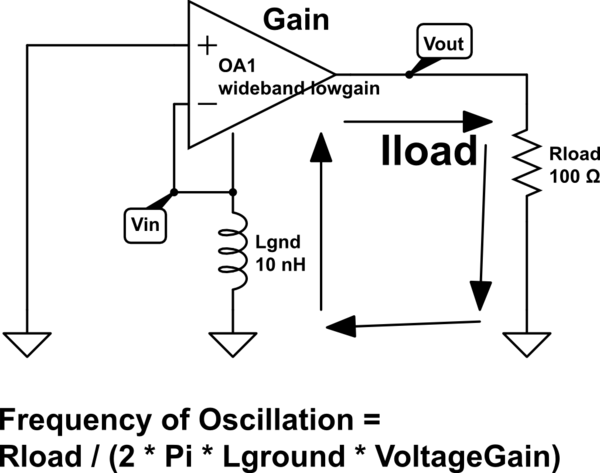
schematic

simulate this circuit – Schematic created using CircuitLab

Notice the Iload flows back into the Amplifier thru the SINGLE GROUND pin, which has inductance.

Given the input signal (Vin+) is grounded, we may wonder what is going on. However, that input signal is between Vin+ and Vin-, which is tied to the Return path of the high output current.

Which is on the top of an inductor, thus that "input signal" will be rising as the frequency rises.

At some high frequency, that Vground (or the Vin-) will be large enough to cause oscillation.

Let's run the math:

Vout = Vin * Gain (and we assume Gain is flat, for easy derivation)

Vin = Lgnd * d(Iground)/dT

Iground = Vout/Rload

Vin = Lground * d(Vout/Rload)/dT

and assume Vin and Vout are sinusoids, thus

Vin = Lground/Rload * d(Vout*sin(2*pi* Freq *time))/dT

Vin = Lground/Rload * Vout * 2 * pi * Freq *cosine(2 * pi * Freq * time)

and picking the peak amplitude, we have

Vin = Lground/Rload * Vout*2*pi*Freq

and we can replace Vout by Vin * Gain, to find

Vin = Lground/Rload * Vin * Gain * 2*pi*Freq

So we manipulate this, to find

1 = Lground/Rload * Gain *2*pi*Freq, and now solve for Freq(of oscillation)

Rload/(2*pi* Lground *Gain) = Frequency of oscillation

What is the frequency (of possible oscillation, ignoring phase shift) if Rload = 50 ohms and Lground is 10nH and Gain = 1 ???

Frequency = 50 / ( 6.28 * 10nH* 1) = 50 / 63nano

Frequency ~~ 800 Megahertz

Which means what?

That RF transmitters should have differential outputs.

===========================================

Suppose you have gain of 10,000 (Flat) and 100nanoHenry inductance, and 1Kohm resistance.

What is your risk of oscillation?

Fosc = Rload / (6.3 * Av * Ground Inductance)

Fosc = 1,000 / (6.3 * 10,000 * 0.1uH)

Fosc = 159 / (10,000 * 1e-7) = 159 / 1e-3 = 159KHz

How does the designer prevent this?

By keeping Load Currents away from the inputs.

By using Bypass Capacitors. By using multiple stages.

==================================

Sometimes two capacitors in parallel will resonant. Plan to dampen them.

What is the application of capacitor between Vcc and GND

\$\endgroup\$
2
\$\begingroup\$

There are four basic answers to this question:

  1. If you don't know what you are doing or have no time/budget to figure out all the intricacies of the design, use them in every single supply pin. No exceptions. It is the most likely path to success.
  2. If you know what you are doing. At least for some sections of the circuit, you can optimize values and placements and might choose to use more or less decoupling as needed.
  3. Chip designers generally should know what they did, they are very likely to apply (2) on writing their data sheets, follow their recommendations to override (1)
  4. If, after following (1) and (3) you have to debug a nasty problem, make the time and apply (2).

Depending on how the different PCB impedances affect the circuitry connected to every supply pin, an IC or design might be more or less sensitive to decoupling on specific pins and supplies. Current paths to different supplies could have different effects on circuit behavior. Being very generous with decoupling is a rather inexpensive way to ensure that a circuit works on first try. But this is not always the case, see this answer for some details.

In some cases there is such thing as too much decoupling. You can actually introduce unwanted resonances on a circuit by using the wrong kind of decoupling. I am just in a middle of a design in which excessive decoupling (due to the use of ceramics for space saving in bulk capacitance) can cause large voltage overshoots on a supply or even large voltage oscillations, bringing dangerous conditions to the circuitry. I had to actually make the decoupling worse (by adding series resistance) to avoid this condition, this is a node that I will pay close attention to when the prototypes come back.

I once had to debug a nasty intermittent problem on a TI power controller that would stop working after a couple of hours, requiring a reset. This took more than a man-month to figure out, and required contacting TI support multiple times. We finally figured out that the problem was really an IC design flaw that imposed an extremely tight ripple tolerance on one specific reference pin, it needed a rather large decoupling capacitor on top of the pin itself, place it just 1mm away (as we had done) and it would cause this problem.

\$\endgroup\$
1
\$\begingroup\$

Using these capacitors depends to your design. If your components and your design may tolerate noise on supply pins, and voltage drop on that supply pins not affects your design, you don't have to use. 100 nano-farad is just a good common value for decoupling.

  • If you want to filter high frequency noise on supply pin use low capacitance capacitors. Sometimes pico-farad capacitors used in RF components to filter realy high frequency noises.
  • For low frequency noise, you need to use high capacitance. For example some micro-farads especially for regulators. BTW using higher capacitors helps you to tolerate transient voltage drops because of the transient currents. These are generally written on datasheet.

In short capacitor value changes according to your circuit design.

\$\endgroup\$
1
\$\begingroup\$

They are best used when the IC manufacturer's data sheet recommends you use them. And connect them in the way that the IC manufacturer recommends - usually close to the supply pins.

Don't skimp in capacitors just to save a few cents just because some parts of the circuit are "less important".

\$\endgroup\$

Your Answer

By clicking “Post Your Answer”, you agree to our terms of service and acknowledge you have read our privacy policy.

Not the answer you're looking for? Browse other questions tagged or ask your own question.