I am trying to listen in on a SPI-like protocol which is transferred on one busline in both directions (no slave-select). To discriminate which data is sent by which side, I need a bus splitter that transmits the data but lets me see which side it was generated on. The bus idles on high on 5V and is pulled low by either side for clocking out bytes at 156kHz.
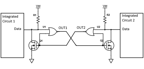
I found the following design online (fig. 6) and implemented it on a bread board. For R1 I used 10kΩ. The NOR-gates are TI SN74HC02 and the MOSFETs are ON Semiconductor BS170 (I used BJTs before which resulted in too much of a voltage drop). The power source/groudn level is driven by the master device so that all voltage levels match with the other bus lines (which I do not need to split).
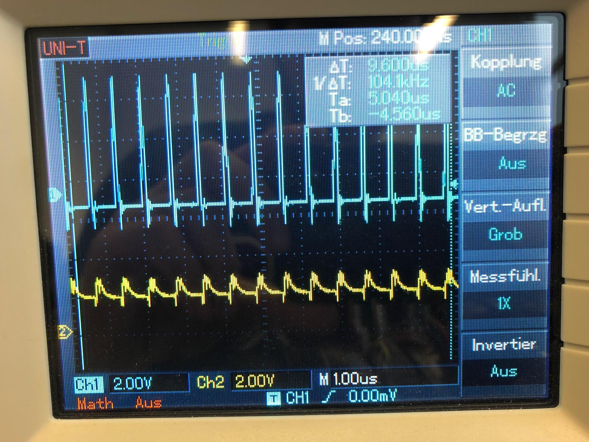
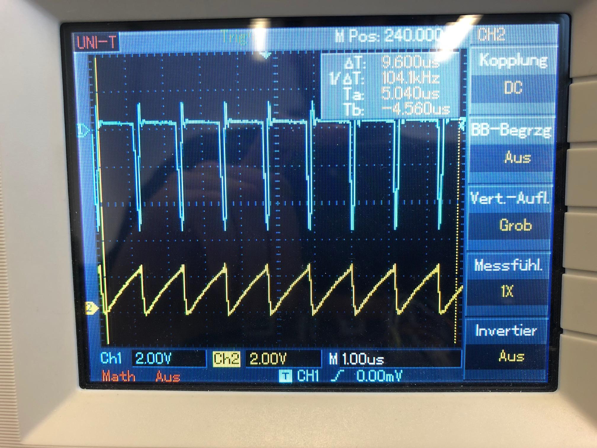
Going over it with a multimeter/Arduino testing program, everything seemed to work okay. When I inserted the circuit into my bus line though, the slave would not be identified by the master anymore. For debugging I set up function generator and oscilloscope and tried to simulate the square wave type signal. Curiously enough, when I applied idle high state on IN1, its voltage would be reduced to around 2.5V, the OUT2 would see sharp peaks to low (otherwise idling on high) and the IN2, where the data from IN1 should be transmitted to in an transparent manner, was a saw tooth. The same behaviour appears with the actual apparatus just idling on high, there is no signal going on here, yet there is an oscillation
IN1 is set to 5V, others floating. Ch1 (blue) is OUT1 (where there should be the inverted signal of IN1), Ch2 is IN1 (which should be steady at 5V

In this picture same setup, IN1 to 5V, others floating. Ch1 is OUT2 (which should low as it inverts the free state of IN2) and Ch2 is IN2 (which should be the signal from IN1, thus high.

Why is the device not working as advertised? I thought the description of it made sense. While looking up flip-flops on Wikipedia I noticed that the device basically is two flip-flop designs thrown together, and that flip-flops might generate these oscillations.
I also added various resistors at U1/2 or between the MOSFET and Q1/2 or between the gat of the MOSFET and GND, to no success. I generally don't have much knowledge of electronics and am just hopelessly puzzled. Does anyone recognize the mistake or can point me to another working design for this type of device?

