0
\$\begingroup\$

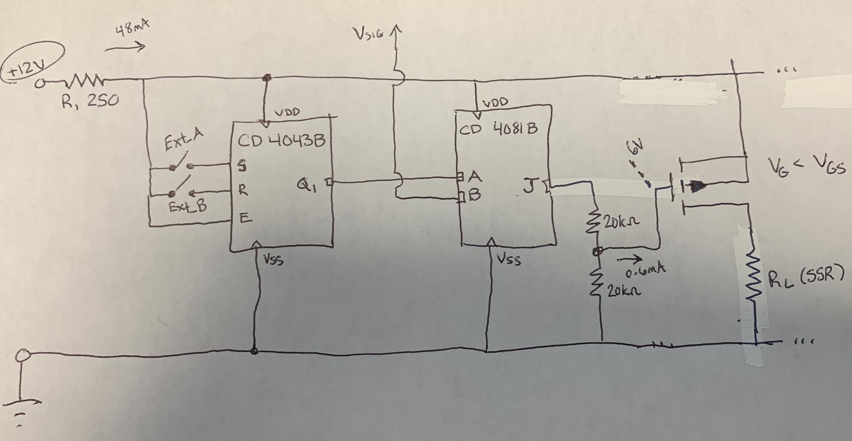
I am attempting to implement a latching circuit without software. The results thus far seem promising, but now I want to drive a control line on a solid-state relay using its output as a high-side PNP switch. I opted to use some CMOS logic ICs to simplify the construction of the circuit, so I want to feed one of the IC's output to the gate of a PFET. These CMOS ICs have limited current output, so I thought to try a simple voltage divider to both A.) keep the current output low, and B.) keep Vg negative with respect tp Vs.

Does this design practice seem feasible? If not, what are some recommendations?

ICs: CD4043B cmos r/s latch CD4081B cmos and gate

EDIT: Schematic should read "Vg < Vs" or in this case basically 6V<12V

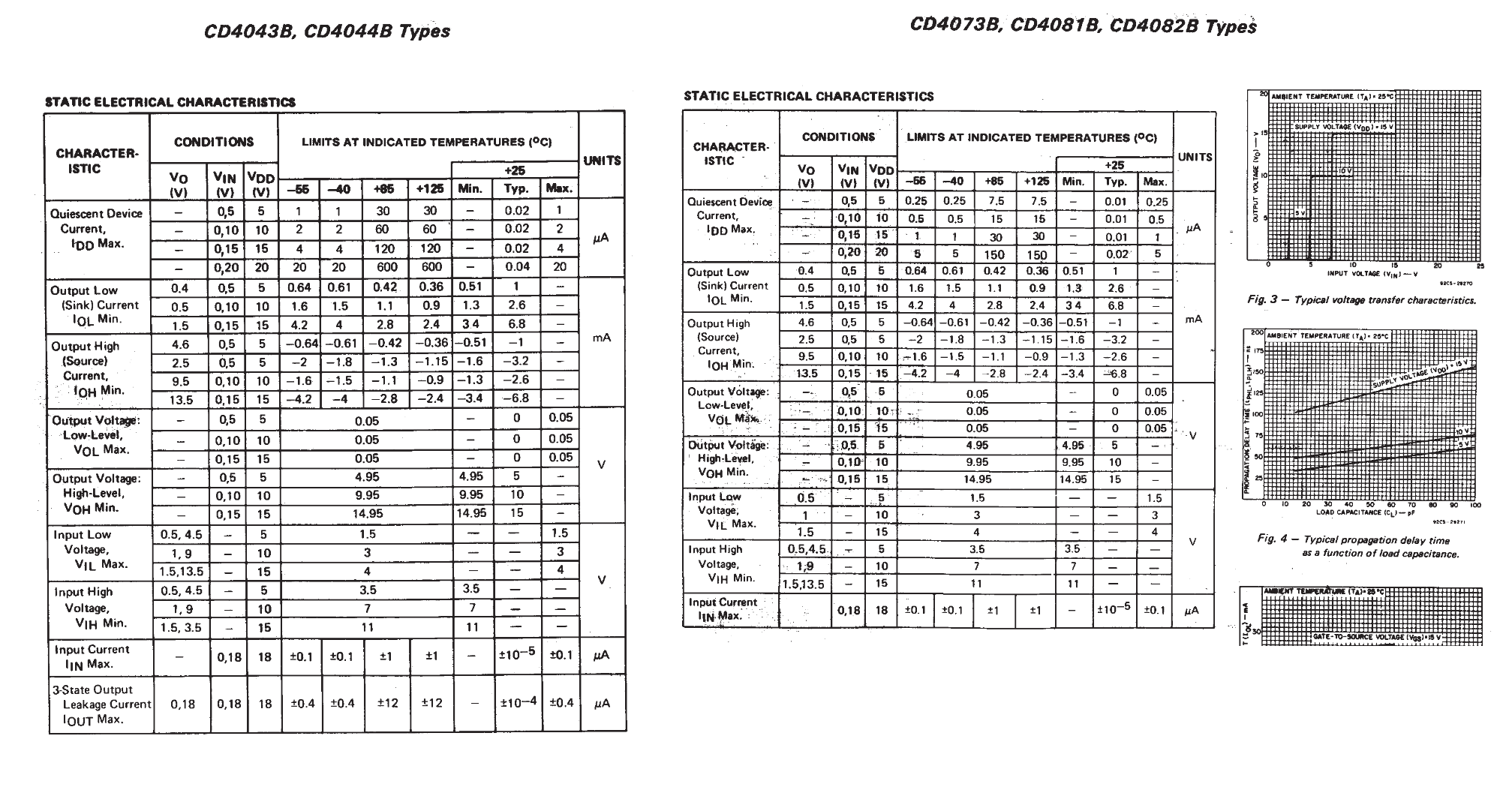
Circuit CMOS datasheets

EDIT 2:

Truth tables for the CD4043/4044
Proposed pfet inverter

\$\endgroup\$
6
  • 1
    \$\begingroup\$ Your 4043 needs pulldown resistors to Vss on its R & S inputs (try 10k). Your 20k resistors need to return to Vdd NOT ground (when the 4081 is HIGH, you want Vgs to be ZERO so the MOSFET is off). With these changes, the load will see +Vdd when the MOSFET is "on" and NO pull-down (basically, open circuit) when it's off -- will that work, given the input specs of your SSR? \$\endgroup\$
    – Atomique
    Commented May 18, 2020 at 19:59
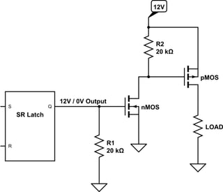
  • \$\begingroup\$ I see the problem in your circuit. Disconnect everything from the Q output, even the 20k resistors. Now, connect Q to the nMOS gate and a 20k resistor from the nMOS gate to GND. Connect the nMOS drain to the pMOS gate. Also from the pMOS gate connect a 20k resistor up to VCC. Leave the load (SSR) as like you have it. \$\endgroup\$
    – Big6
    Commented May 26, 2020 at 0:02
  • \$\begingroup\$ Forgot to add, connect the nMOS source directly to GND no need for the 47k resistor, unless you're concerned about over-voltaging the pMOS. And don't connect the nMOS drain to the Q output, like you did in your circuit. \$\endgroup\$
    – Big6
    Commented May 26, 2020 at 0:22
  • \$\begingroup\$ This simulates pretty good! Can't seem to mark this comment as solution, though! :( Thanks for the suggestions, Big6. \$\endgroup\$
    – Big Owls
    Commented May 26, 2020 at 3:53
  • 1
    \$\begingroup\$ I edited the answer to reflect the changes I suggested in my comment \$\endgroup\$
    – Big6
    Commented May 26, 2020 at 4:13

1 Answer 1

1
\$\begingroup\$

You have a PFET at the output instead of a PNP, so you should not worry about any current going into the PFET's gate. Sure, there is a current (i.e gate charge) that flows into it when turning it on or off and that mainly determines how fast you can operate the PFET.

Now, in the configuration you show, the PFET will always be ON. That is the case because at the output of the CD4081, you can either have a '1' (~12V) or a '0' (0V). The PFET turns on when \$V_S\$ is at a sufficiently high potential with respect to \$V_G\$. Say the output of your CD4081 is at 12V, then \$V_G=6V\$ and \$V_S=12V\$, so \$V_{GS}=-6V\$, that is good enough to turn on lots of PFETs. If on the other hand, the output of your CD4081 is at 0V, then \$V_G=0V\$ and \$V_S=12V\$, so \$V_{GS}=-12V\$, again, that is good enough to turn on most PFETs.

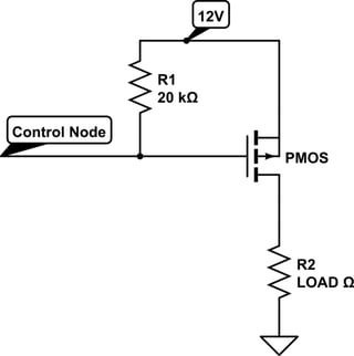
You really want to do something like this with your output PFET:

schematic

simulate this circuit – Schematic created using CircuitLab

The control node is the output of the CD4081. When high (12V), \$V_{GS}=0V\$ and the PFET is OFF. If the control node is low (0V), \$V_{GS}=-12V\$, and the PFET is ON, and the load will see 12V across itself.

EDIT:

I looked at the circuit you linked and I see what you did wrong. This is what you really want to do:

schematic

simulate this circuit

\$\endgroup\$
7
  • \$\begingroup\$ I'll consolidate my remarks for both you and Atomique's answer here, as I think they are similar in response. I do indeed have the pull-downs on S and R. They are actually 1M resistors because that's what was advised in the TI documentation for the product. Sorry for omitting that. Regarding these suggestions, thank you! I understand for the most part what needs to be done, but I am still hung up on the 4081's output. I intended / expected that to be +12V when activating SSR. Can this be done, or does it need to be inverted? Does that mean additional components or a different (NAND?) IC? \$\endgroup\$
    – Big Owls
    Commented May 18, 2020 at 23:34
  • \$\begingroup\$ @user8585939 You can do two things: Option1) Replace the PFET with an NFET, but you now need to move your load "up" and use the NFET to switch the GND instead of the +12V, as you are doing with the PFET, google NMOS low side switch. Option 2) Keep the circuit as is but use an extra transistor, an NFET. Connect the NFET's drain to the "control" node shown in my answer, the NFET's source to GND, and its gate to the 4081's output. That way your PFET will still switch the high side (+12V) to the SSR and the NFET will work as an inverter. Hope that makes sense. \$\endgroup\$
    – Big6
    Commented May 19, 2020 at 0:35
  • \$\begingroup\$ The CD4043 has a NAND-gate equivalent which I suspect was purpose-built for this type of circumstance, which I have edited the post to include above. The only thing I don't seem to be quite clear on is why the NAND CD4044 IC would be designed such that if S=0 and R=0, it leaves Q to be dominated by the 'R=0' input. It seems like that removes a very desirable behavior of this 'latch' circuit to eliminate chatter from one end of the equation. On the 4043, it replaces this behavior with "NC," which allows the system to ride up and down undisturbed after the change in hysteresis. \$\endgroup\$
    – Big Owls
    Commented May 25, 2020 at 20:55
  • \$\begingroup\$ @user8585939 Well, for a NAND based SR latch, the S=0 and R=0 is not an allow state, the same is true for a S=1, R=1 in a NOR based latch. I guess, they just give you some guarantee of what Q will be if that particular combination is asserted. \$\endgroup\$
    – Big6
    Commented May 25, 2020 at 23:06
  • \$\begingroup\$ @user8585939 You can make the circuit simpler by just using a D latch. You will just have one input, D, and an Enable pin, E. The Q output will follow the input D, so long as E is asserted. You can decide what level at the D, will operate the driving FET. If you have a high level on D, Q will be high so an NMOS can be used as a low side switch to power the load. If you want the inverse logic, so that low enables the output FET, you can the use a PMOS as a high side switch. \$\endgroup\$
    – Big6
    Commented May 25, 2020 at 23:08

Your Answer

By clicking “Post Your Answer”, you agree to our terms of service and acknowledge you have read our privacy policy.

Not the answer you're looking for? Browse other questions tagged or ask your own question.