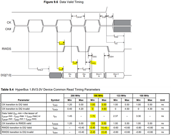
I'm trying to design an interface between an application processor and a HyperFlash memory from Cypress. Therefore, I'm trying to understand the timing diagram for RWDS and DQs relative to the CLK line. Here is the timing diagram representing the valid and invalid areas of the given signals:
(Clock frequency is set to 166 MHz and the operating voltage is equal to 1.8V)
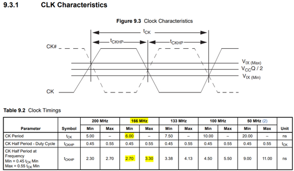
This is how the clock signal looks like:
I am trying to recreate the timing diagram using a third-party application, to design the interface to guarantee the minimum setup and hold timings etc. Here is how it looks like: (Measurement level is VccQ/2)
I have created 2 scenarios, based on the datasheet values and both seems to be incorrect.
The first is where the RWDS valid region (t_CKDS) tracks the CLK transition on both edges. That's how I understood at first, according to the datasheet. However, in this scenario, the valid area of the RWDS signal is nonexistent. Minimum time to the RWDS valid is specified as 1 ns, the maximum is 5.5 ns, relative to the CLK. Well, the positive and negative clock width is equal to 3 ns typical (let's ignore any jitter etc.). So, until the next transition of the CLK, there isn't enough time for the RWDS to be valid. Same is applied to the DQx lines in this example.
In the second scenario (since the first one failed), I drew the t_CKDS only on the rising/falling edge of the CLK/CLK# signal. That gives the RWDS a valid area of 1.5 ns. However, it should be minimum 2.46 ns, according to the xSPI specification as far as I am concerned. Also, this gives the DQx signal a valid area of 600 ps maximum. On the datasheet the data valid has a minimum value of 1.7 ns (t_DV).
It seems like to match the datasheet timing (read operation, t_CKDS, t_CKD, t_CKDI, t_DV, t_DSS, t_DSH) values, the clock frequency must be around ~65 MHz maximum. However, the values are listed for 133 MHz operation.
Plus, the CK transition to DQ/RWDS valid time delays appear to be fixed over the whole frequency of operation range. Could it be really fixed or is it more of a print mistake in the datasheet?
Obviously, I am missing something here. I'll be glad if anyone experienced can be of any help and point that out. How to interpret this timing diagram with the given values? What is the reason for the timing mismatches here? Thank you.


