1
\$\begingroup\$

I started building basic logic gates. I wanted to start basic and understandable so I started building some NAND gates just using two transistors. On its own hooked up to a switch and a LED they work as they should, so I continued chaining them.

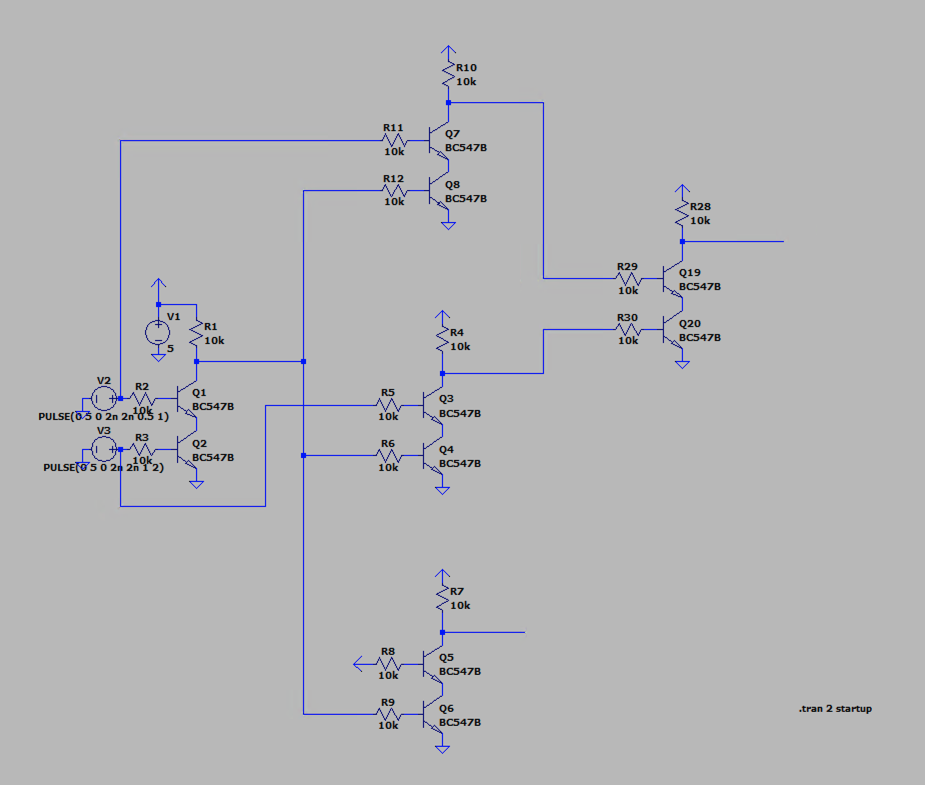
I first tried to simulate this circuit using LTspice where everything looked fine. However testing them out with hardware does not result the same way. I chained 4 NAND gates to form a XOR gate. If I add an extra NAND gate like shown below, the output of the XOR gate does not work anymore.

XOR and NAND gate circuit build from NAND gates

The probes are as follow:

  1. V2
  2. V3
  3. Q19 Collector
  4. Q5 Collector

LTspice simulation result

But my measurements (in V) are (* means using 1k for all pull-up resistors):

V2 V3 Q19 Collector Q5 Collector Q19 Collector * Q5 Collector *
5.00 5.00 0.03 5.00 3.10 4.18
0 5.00 2.22 1.36 3.70 2.88
5.00 0 5.00 0.08 3.33 2.86
0 0 0.03 1.36 2.69 2.88

This is my circuit build on a breadboard (same wire colors are connected together, except the green and red going out of the picture are where I measured the values. And the black and yellow wires are where I set my input signals): Circuit build on breadboard
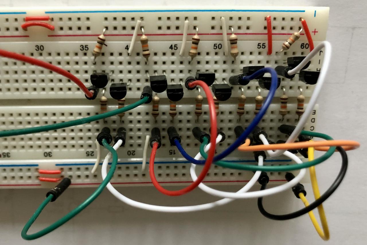
My questions are:

  1. Why is the LTspice simulation wrong (This is my asc file)?
  2. Why does this behave like that and how can I get the gates to work as they should?
\$\endgroup\$
15
  • 2
    \$\begingroup\$ Make your collector resistor smaller (1kΩ). TTL could sink a lot of current, but source depends on pullup resistors. \$\endgroup\$ Commented Mar 5, 2023 at 19:50
  • 1
    \$\begingroup\$ I can test 1k out, but why does this work in the simulation? Isn’t that circuit design called RTL (resistor-transistor-logic)? From what I understand TTL NAND gates use multi emitter transistors and they don’t waste current if both inputs are high? \$\endgroup\$
    – wolflu
    Commented Mar 5, 2023 at 20:17
  • 1
    \$\begingroup\$ I'm too lazy (or tired?) to simulate it, but when the upper transistor has more current gain, \$V_{CE}\$ of the lower one should be higher than that of the upper one, leading to an unwelcome high voltage at the output - enough to "open the next lower transistor". The difference the third input at the first gate output makes is going from a 10k:5k+ voltage divider to 10k:3.3k+, compounding to the problem: output pull-ups should probably be one tenth of input resistors. \$\endgroup\$
    – greybeard
    Commented Mar 5, 2023 at 21:41
  • 2
    \$\begingroup\$ All the transistors on your breadboard are flipped backwards. I think you have C and E mixed up. i.sstatic.net/GUtma.png \$\endgroup\$
    – Ste Kulov
    Commented Mar 6, 2023 at 18:26
  • 2
    \$\begingroup\$ The next step would be to build it incorrectly in LTspice and probe around various voltages and currents to get an idea of how it was operating like that. It's still worth noting that it's best practice with these types of circuits to heed @greybeard 's advice of "output pull-ups should probably be one tenth of input resistors" so you have more stable logic levels as your circuit grows with more NAND gates attached. \$\endgroup\$
    – Ste Kulov
    Commented Mar 7, 2023 at 6:17

0

Your Answer

By clicking “Post Your Answer”, you agree to our terms of service and acknowledge you have read our privacy policy.

Browse other questions tagged or ask your own question.