0
\$\begingroup\$

The TPS63710 is a low noise inverting buck converter capable of a relatively high efficiency conversion from 5V to -3.3V (according to TI's WEBENCH tool), but an aspect of the datasheet's layout guidelines is troubling me. The device requires a capacitor Caux placed between pin VAUX and GND, and moreover it stipulates:

Because Caux carries the peak currents of the gate control block, it should have a compact and direct routing to VAUX and GND pin 10, staying away from sensitive signals.

As you can see on the datasheet's layout image below, instead of connecting Caux immediately to GND, they route an isolated trace back under the device to GND pin 10. Does anyone have any insight/explanation on what purpose this serves? Perhaps there is additional filtering functionality behind pin 10, but it ties into the GND net just under the device anyway, so I'm confused how this accomplishes much. Or am I missing the point entirely? I could find minimal explanation on the rationale in either the datasheet or TI forums.

Also, my board is 4-layers with full GND planes on layers 2 and 3, making it a bit janky to effectively isolate a trace back underneath to pin 10. In this case, do people think the likely benefits still outweigh the additional layout complexity? Is it likely a bad idea to ignore this suggestion and just tie Caux ASAP into the GND plane below?

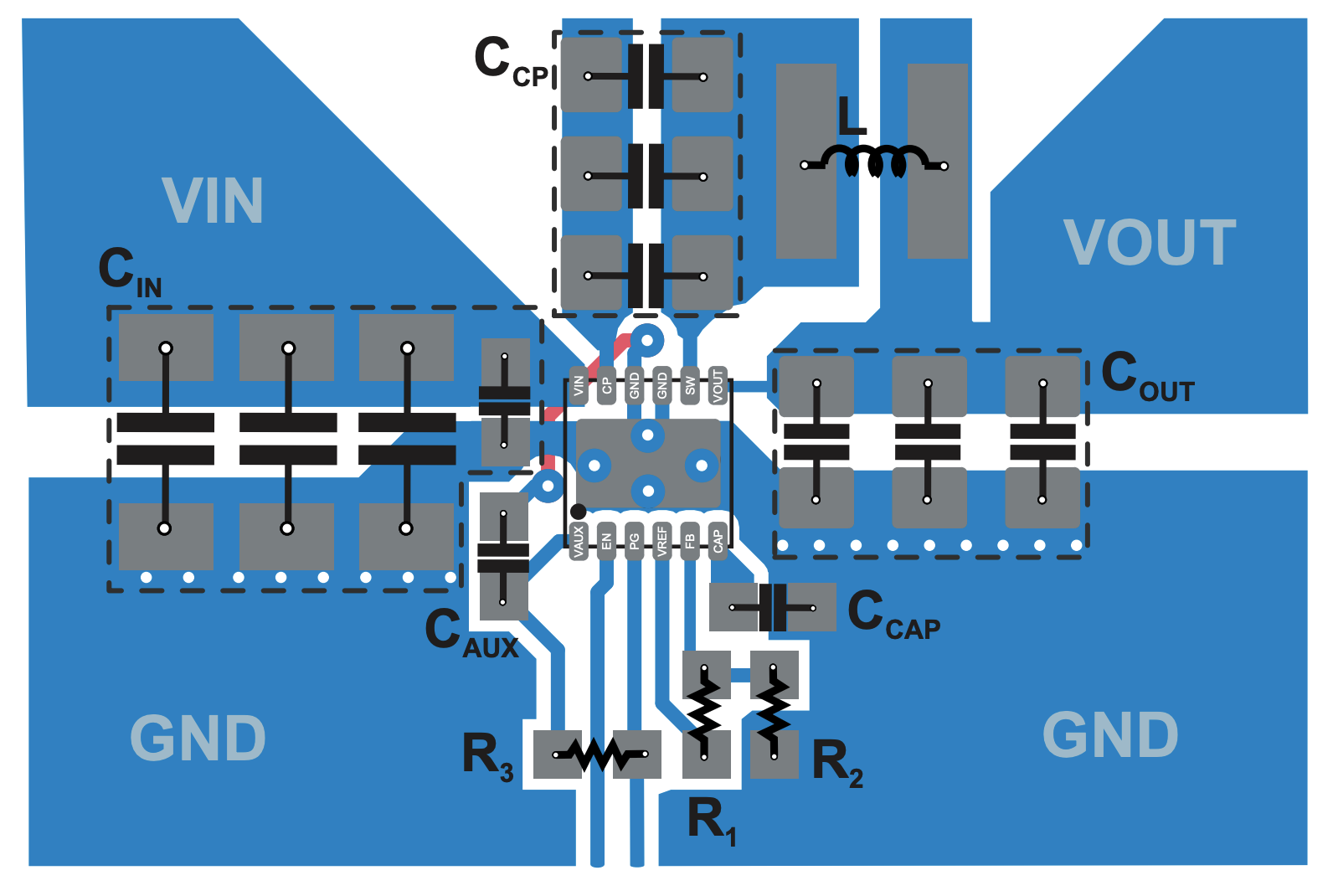
enter image description here

\$\endgroup\$
1
  • \$\begingroup\$ I doubt it makes a difference. You could ask the manufacturer via their forum e2e.ti.com about the justification for it; I expect there's very little we can say about it, unless someone has specifically measured the characteristics of these pins, or explicitly tested contrasting but otherwise equivalent layouts. (Not saying it's impossible, or not worth asking, just that you're more likely to get answers in the correct place.) \$\endgroup\$ Commented Jul 7 at 0:10

1 Answer 1

0
\$\begingroup\$

It's not much different than having a bypass cap on a normal logic IC with one supply and one ground pin.

Or rather, a logic IC with built-in regulator and the logic that uses the output of the regulator. Or in a larger scale, a PCB module with onboard regulator and some MCU, but external connections for connecting the capacitors.

Inside the chip, there may be different sub-blocks powered via different pins. For example, you don't know if the two GND pins are connected inside the chip, or what they are used for. One of them could be a GND pin for sensitive low current analog circuits and the other for high currents from digital switching waveforms.

So it may be that the pin 10 is the GND reference pin of the bias regulator and the VAUX is the output of bias regulator which is also used internally for analog and digital circuits that power the chip.

Therefore it is important that an exteral bypass capacitor connects directly between these two pins, and that no other currents flowing on the PCB can flow in a way that would cause noise or ripple to couple to the VAUX pin, so no other currents can also flow on the copper trace between capacitor and GND pin.

If you instead would just connect the VAUX capacitor ground side to the big ground plane that already runs under the chip, the copper trace will have some resistance, and so switching currents passing on the copper trace will produce a ripple voltage between the pin 10 and capacitor, and the capacitor would couple the ripple to the VAUX pin.

The way the example shows it, no matter how much there is voltage fluctuations at pin 10 due to flowing currents on PCB track, the capacitor is able to keep voltages between GND and VAUX stable so they both fluctuate with regards to the GND pin.

\$\endgroup\$
2
  • \$\begingroup\$ Interesting, do you have measurements of these pins (peak currents, rate, susceptibility)? You say it's important, but how much really matters, what trace width and length will have what kind of effect? \$\endgroup\$ Commented Jul 7 at 0:47
  • \$\begingroup\$ @TimWilliams That is a good question. Often manufacturers suggest you an example layout, and they are just that, suggestions. There may be better or worse layouts and it will affect the performance of the chip or emitted interference or output ripple or whatever - and even a poor layout could do just fine in your application. However, if a manufacturer tells you to specifically put a capacitor weirdly between two pins directly, they have a good reason to say that, and when asked, they will some reason, but in reality, it may just be a workaround for a silicon bug. \$\endgroup\$
    – Justme
    Commented Jul 7 at 8:22

Your Answer

By clicking “Post Your Answer”, you agree to our terms of service and acknowledge you have read our privacy policy.

Not the answer you're looking for? Browse other questions tagged or ask your own question.