Your question is very interesting. It shows a tendency towards deep thought rather than the mechanical application of common textbook clichés.
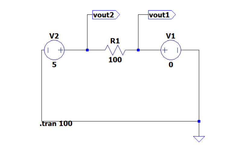
Your circuit is a NOT gate
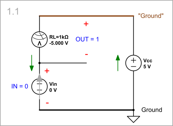
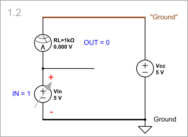
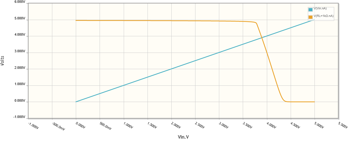
It is indeed a NOT gate if the output voltage (the voltage drop across resistor R1) is measured with respect to the positive rail of V1. In fact, this voltage is the complement of V1 to V2, which in this digital circuit represents its negation. Let's draw the circuit in its conventional form and analyze its behavior for both possible input voltage values (0 V and 5 V). Your R1 resistor is represented by a real voltmeter with 1 kΩ internal resistance acting as a load; hence the odd name "RL=1kΩ".
Vin = 0 V ("0"), Vout = 5 V ("1")

simulate this circuit – Schematic created using CircuitLab
Note that since referenced to Vcc the output voltage across the load RL is negative.
Vin = 5 V ("1"), Vout = 0 V ("0")

simulate this circuit
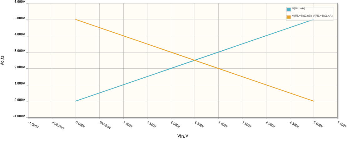
Analogously, in an analog circuit like a common-emitter, the voltage across the collector resistor (in orange) is the complement of the collector voltage. We prefer to use the collector voltage since it is referenced to ground.

Why do we not consider this circuit and instead use transistors in practical NOT gate ICs?
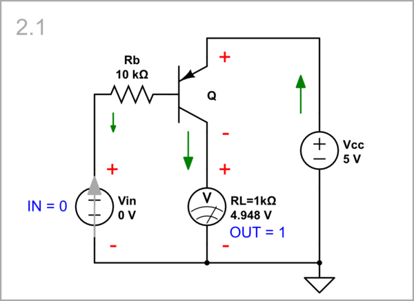
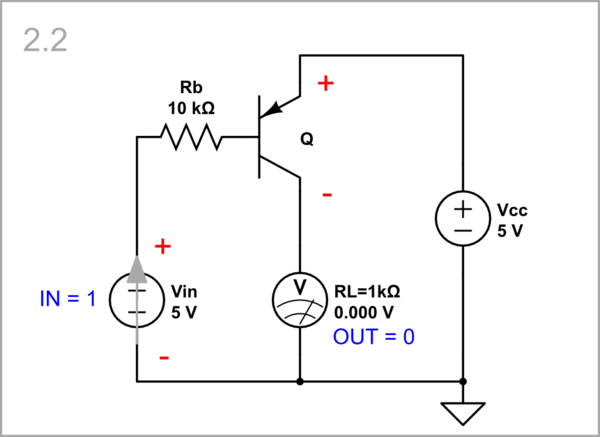
However, in circuits, we prefer to refer signals to ground because this simplifies the connection between stages and the measurement of voltages. So, we have to feed the signal back to ground (e.g., with a PNP transistor) by "folding" the circuit.
Vin = 0 V ("0"), Vout = 5 V ("1")

simulate this circuit
Vin = 5 V ("1"), Vout = 0 V ("0")

simulate this circuit

Voltage as a data carrier
For this purpose, voltage, rather than current, is used as the carrier of information in logic gates as well as in most analog circuits. This allows us to connect input-output ports in parallel (cascade) with respect to ground.
NOT gate as a "voltage divider"
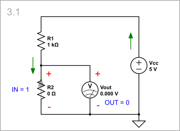
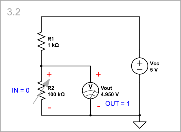
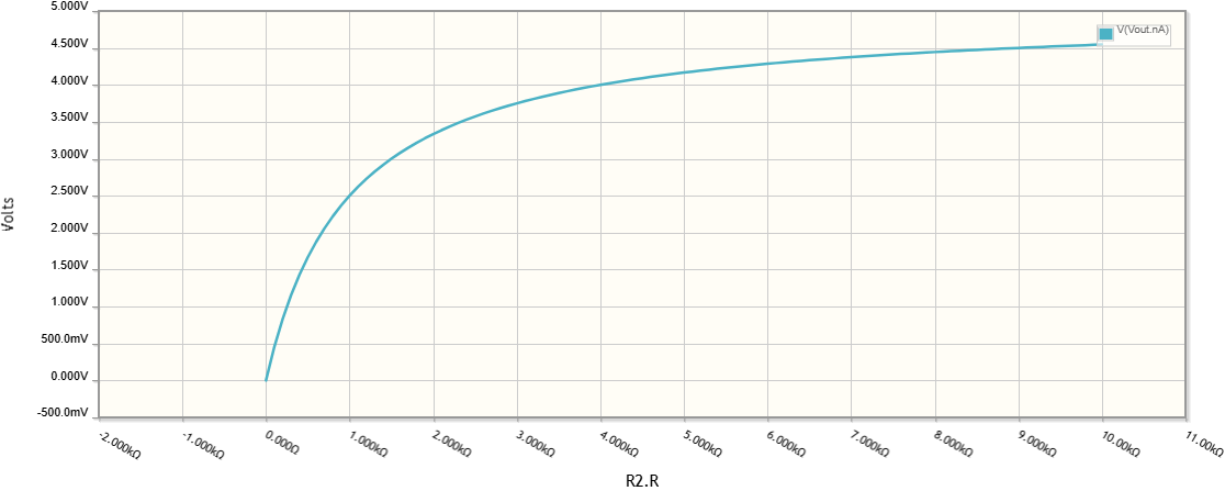
Conceptual circuit. Thus, logic gates deal with voltages, and the device with which voltages are controlled in the most general case is a voltage divider. It consists of a "pull-up" element (e.g., resistor R1, switch SW1, PNP transistor Q1, etc.) and a "pull-down" element (e.g., grounded resistor R2, switch SW2, NPN transistor Q2, etc.). The most general property of these elements is that they have resistance (no matter linear or non-linear). In the simplest case, they are represented as voltage-controlled switches with infinite resistance when open and zero resistance when closed. Let's explore this conceptual circuit by CircuitLab.
Vin = 5 V ("1"), R2 = 0, Vout = 0 V ("0")

simulate this circuit
Vin = 0 V ("0"), R2 = 100 kΩ, Vout = 5 V ("1")

simulate this circuit
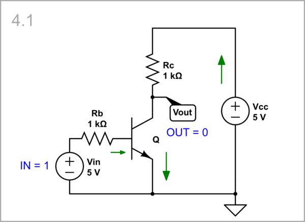
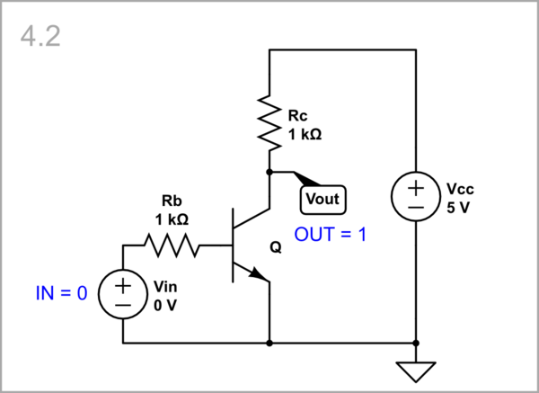
BJT implementation: Let's now explore the classic BJT NOT gate implementation.
Vin = 5 V ("1"), Q on, Vout = 0 V ("0")

simulate this circuit
Vin = 0 V ("0"), Q off, Vout = 0 V ("1")

simulate this circuit
When does this configuration invert?
In order for the input and output voltages to be relative to ground, it is simplest to control the resistance of the lower element. If the dependence between the input voltage and the resistance is inverse (aka "enhancement type"), with an increase in voltage, the resistance will decrease and the voltage drop across it (the output voltage) will also decrease. As a result, the circuit will invert, i.e., it is a NOT gate.

Why can't a NOT gate be made with diodes?
Why can we not make NOT gates using diodes and resistors...
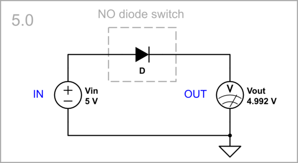
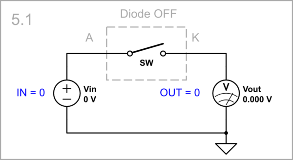
In principle, diodes are switches but 1-port; they have only two terminals that are both input and output (unlike transistors which are 2-port, with separated input and output). While conventional 2-port switches are connected in series with a constant voltage source (Vcc), diode switches are connected in series with the varying input voltage source. This does not allow a NOT gate to be made with them. Let's explore it by CircuitLab to see why.
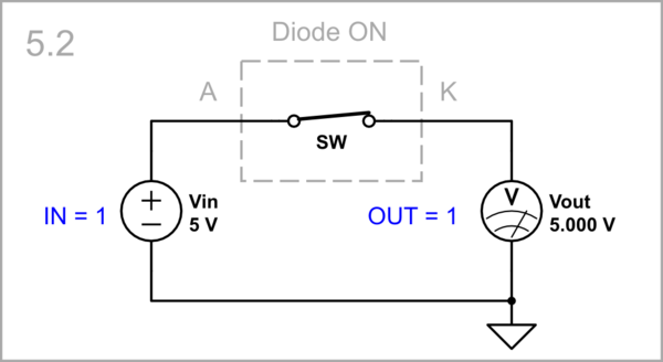
Forward-connected diode: If the input voltage source is connected to the anode...

simulate this circuit
... and Vin = 0 V, the switch is off and Vout = 0 V.

simulate this circuit
If Vin = 5 V, the switch is on and Vout = 5 V. So, this diode circuit is not an inverter (NOT gate) but a follower.

simulate this circuit
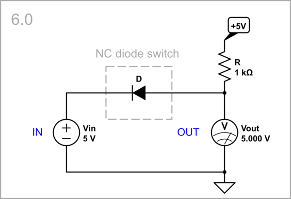
Backward-connected diode: Then let's try to connect the input voltage source to the cathode ("pulling up" the anode by a resistor R to 5 V).

simulate this circuit
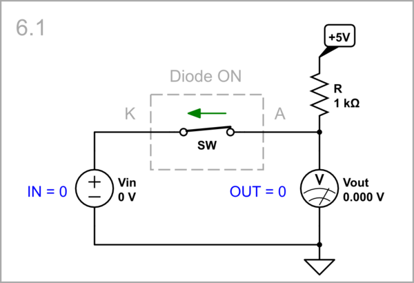
Now, if Vin = 0 V, the switch is on and Vout = 0 V. Note that the current enters the input voltage source (basic property of DTL and TTL gates).

simulate this circuit
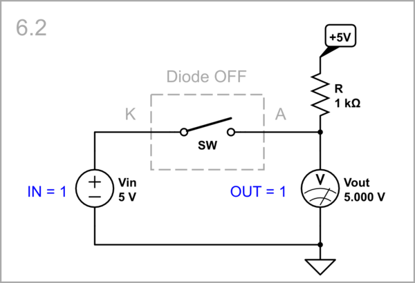
If Vin = 5 V, the switch is off and Vout = 5 V. Again, this diode circuit is not an inverter (NOT gate) but a follower.

simulate this circuit
Thus, in both diode configurations, the diode switch directly connects the input source to the load, resulting in a non-inverted output voltage.
... just like we do in OR and AND gates using Diode-Resistor Logic?
However, these diode circuits are useful when there are multiple input sources (in OR and AND logic gates) because they isolate them. More specifically, in the first (OR) circuit, the diode allows the input source to connect to the load only when there is a positive input voltage, while in the second (AND) circuit, it allows the connection only when there is zero input voltage. Figuratively speaking, the diodes have made the two sources unidirectional - in the first case, the source can only provide (source) current, and in the second case, it can only receive (sink) current. This prevents conflicts between the input sources when they have different voltages.

