2
\$\begingroup\$

I have a signal around 20 V peak-peak. I want to feed it into an emitter follower BJT and I have no experience in working with such large signals.

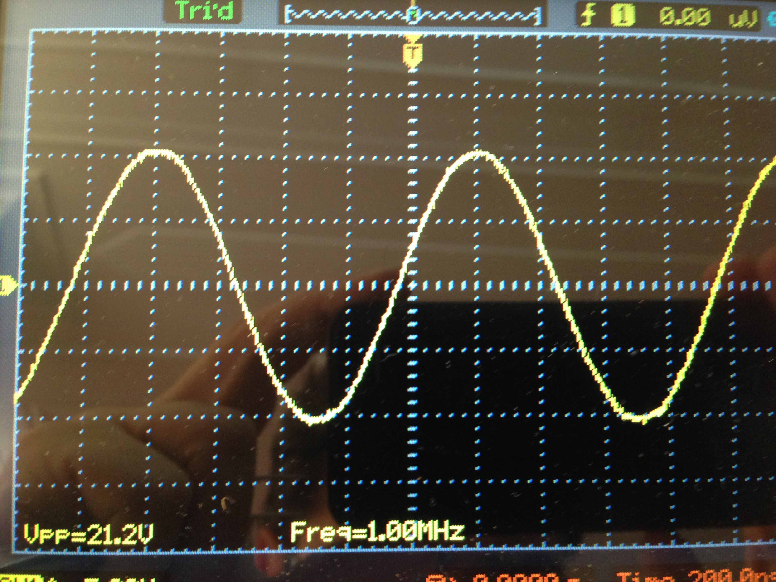
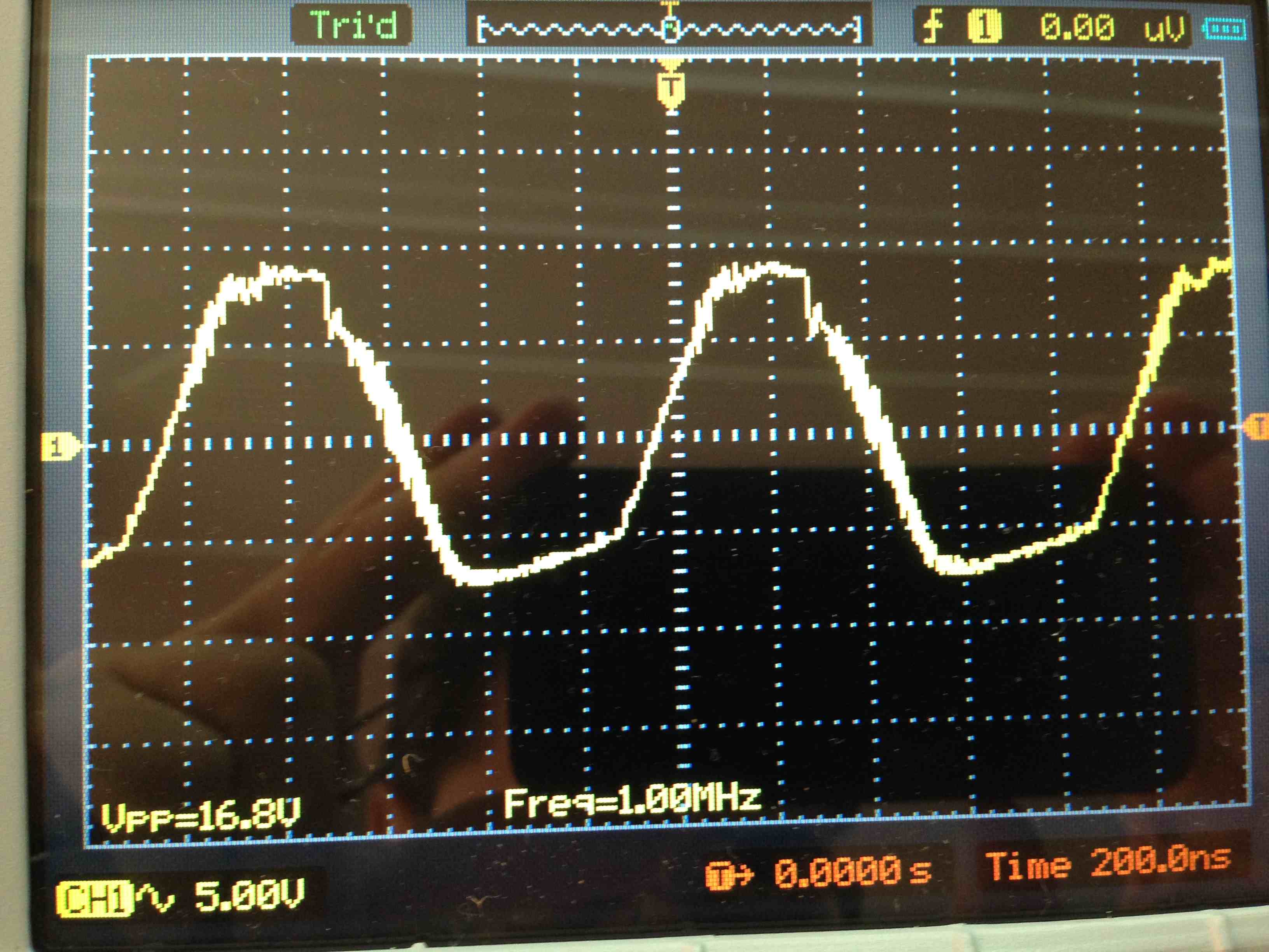
The BJT is well in bias point ( I tested the emitter DC voltage= 15 v with VCC=30V) , the result is awfully noisy and distorted. I included photo of input signal and the output. The frequency can be read on lower left corner of the photos and first issue is a voltage drop.

The second issue is the flat bottom of the output as if it is not well in bias point but it is well biased. I thought about the VCC but a VCC=30v should well handle a 21.2v signal ( at leats I think so).

For testing the bias point, I replaced the base resistor with a potentiometer . By turning the Pot, no better result found.

I tried many BJTs like 2N2219, BC108, BC109A , all the same result ( best result was with 2N2219). All are with moderate speed and transition frequency around 120-300MHz.

The frequency is not a main concern here as I tried many frequencies between 1Hz - 50MHz. Surprisingly the noise was far less in higher frequencies !!!

The design is not a complicated one, just a simple emitter follower (there is a typo, VCC is 30V ).

I put a photo of the input signal ( voltage can be read at left lower corner of the oscope screen and freq in the middle) and a photo of the result:

EDITION: by reducing the input signal amplitude to 10vpp, everything goes well in low frequencies (<10MHz) but distortion gets worse in high frequencies. This may mean that the problem is with large signal size and I may need a faster BJT. How should I handle large signals?

1-Schematic ( VCC is 30 volts ) :
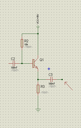
enter image description here

2-Input signal 21.2v 1MHz:

enter image description here

Output: enter image description here

\$\endgroup\$
7
  • 1
    \$\begingroup\$ What kind of capacitor are you using? The distortion may be caused by a Y-rated capacitor (as in Y5R or something). NP0 or X7R would be a better choice in that case. \$\endgroup\$
    – user36129
    Commented Oct 14, 2013 at 11:01
  • \$\begingroup\$ @user36129 simple ceramic 100nF.(through hole ) \$\endgroup\$
    – Aug
    Commented Oct 14, 2013 at 11:03
  • \$\begingroup\$ I got that, but exactly what type ceramic? \$\endgroup\$
    – user36129
    Commented Oct 14, 2013 at 11:28
  • 2
    \$\begingroup\$ What value for R3 and without a signal, what dc voltage is the emitter giving? \$\endgroup\$
    – Andy aka
    Commented Oct 14, 2013 at 11:41
  • \$\begingroup\$ With a Vcc of 30 volts, and an input swing of 20Vpp, you may just be swinging the transistor out of its linear region. \$\endgroup\$ Commented Oct 14, 2013 at 17:32

4 Answers 4

11
\$\begingroup\$

Emitter followers are perilously close to being UHF oscillators; it is quite possible for them to start oscillating during only a small part of the wanted signal cycle; this appears as periodic noise and may also cause the observed distortion. (It is usually too high frequency to observe on a scope!)

The usual cure is a small value resistor (experiment with 22 and 47R) in series with the base, (aka "base stopper") as close to it as possible.

What happens is that the device capacitances in conjunction with the inductance of the base connection cause a parasitic series-resonant circuit, and Cbe provides positive feedback, the emitter current providing the power. The base stopper lowers the Q of the resonant circuit to prevent oscillation.

(It is also possible, as Andy AKA is hinting, that R3 is too high in value and this is clipping the -ve peaks)

\$\endgroup\$
2
  • \$\begingroup\$ This base stopper is between Rb and base? \$\endgroup\$
    – Aug
    Commented Oct 14, 2013 at 18:20
  • 1
    \$\begingroup\$ Yes. More importantly, between C2 and all other external wiring (inc. Rb) and base. \$\endgroup\$
    – user16324
    Commented Oct 14, 2013 at 19:01
2
\$\begingroup\$

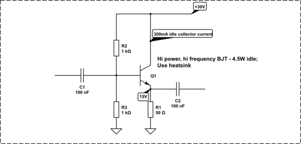
If you want to use simple emitter follower, you must design it properly. You need big idle collector current and low emitter resistance. In the base there must be a voltage divider. The BJT must be powerfull enough to handle this working point:

schematic

simulate this circuit – Schematic created using CircuitLab

The proper solution here is to use more complex push-pull schematic. It will be much more efficient.

\$\endgroup\$
1
\$\begingroup\$

Your emitter follower circuit won't work with a 21Vp-p input - it's only supplied from 0V and +15V. Try changing the emitter resistor to 220R and connecting it to the -15V supply. Directly couple your signal into the base - this assumes that your signal is centred around 0V.

OK I've seen you mention that Vcc is 30V - nevertheless follow what I have said to see what happens and if necessary try Brian's 22R in series with the base. Screen shots at highest frequency and smaller signal level and bigger signal level would be good.

\$\endgroup\$
0
\$\begingroup\$

Your circuit exhibits gross distortions with a high input signal because its peaks are past the supply rails. The amplifier is powered from 15 V but the signal spans 20 V. How did you expect this to work?

Smaller signals, like your 10 Vpp case work because the output fits within the supply limits, so the circuit can operate as intended over the whole voltage span of the signal.

There are probably two reasons the output looks cleaner at very high frequencies. First, there is always stray capacitance between various nodes. This stray capacitance is working against the impedances in your circuit to form low pass filters. Put another way, this circuit can only pass signals up to some maximum frequency. Above that, the signals get progressively more attenuated. This means that when you feed in a signal near the frequency limit, its harmonics, or any harmonics caused by distortion, are attenuated more than the fundamental. This low pass filtering effect reduces distortion.

Second, you may be hitting the limit of what your scope can show you. Perhaps more distortion components are there, but the scope is applying the low pass filtering so that you don't see them.

\$\endgroup\$
3
  • 6
    \$\begingroup\$ The author mentioned the experimental circuit is powered by 30V DC actually. \$\endgroup\$
    – johnfound
    Commented Oct 14, 2013 at 13:22
  • \$\begingroup\$ @john: The schematic clearly shows 15 V. Admittedly I didn't read the whole question, but the schematic should be able to stand by itself. \$\endgroup\$ Commented Oct 14, 2013 at 13:35
  • \$\begingroup\$ Stray capacitance is what i never noticed. Is there any solution to avoid them? Also my oscope is a 200 MHz one and the frequency is not near its limits. Sorry for typo in the schematic. I will correct it ASAP \$\endgroup\$
    – Aug
    Commented Oct 14, 2013 at 18:25

Your Answer

By clicking “Post Your Answer”, you agree to our terms of service and acknowledge you have read our privacy policy.

Not the answer you're looking for? Browse other questions tagged or ask your own question.