8
\$\begingroup\$

I2C uses open collector outputs. FPGAs do not have such outputs. They do have tri state buffers though.

  1. How should open collector output be defined in a VHDL for an FPGA?
  2. How should open collector output be pulled high in testbench? i.e how model the pull up resistor e.g on SDA line that connects master to slave, in a testbench?
\$\endgroup\$
2

3 Answers 3

12
\$\begingroup\$

FPGAs have tri-state outputs :

sda <= 'Z' when dout='1' else '0';

There are also sometimes optional internal pull-ups, but they are not meant to drive external circuits, so an I2C bus will need an actual pull-up resistor.

VHDL std-logic type has 'H' and 'L' values to simulate pull-up and pull-downs. You can write

sda <='H';

in the test-bench to simulate a pull-up.

std_logic is a "resolved" type, a signal can have several drivers, and a resolution function is used to determine the final state : 'Z' + 'H' = 'H' , '0' + 'H' = '0'

\$\endgroup\$
2
  • \$\begingroup\$ But is 'Z' + 'H' = '1'? This is the confusing part. In other words, if both receiver and transmitter are driving 'Z' onto SDA and then one of them reads the value on SDA, it should get '1' since it is pulled high externally right? \$\endgroup\$
    – quantum231
    Commented Jun 14, 2019 at 4:54
  • 5
    \$\begingroup\$ Z + H = H. But to_01(H) = 1, so H is seen as 1 by just about any subsequent gate or process. \$\endgroup\$
    – user16324
    Commented Jun 14, 2019 at 9:55
7
\$\begingroup\$

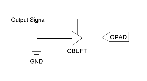
1) According to Xilinx, creating a tristate device in VHDL will help you model an open collector/drain output using the following logic diagram:

enter image description here

The VHDL code:

dout <= 'Z' when din='1' else '0';

The Verilog code (even though you specifically asked for VHDL):

always @(ENABLE)
if (ENABLE)
DOUT = 1'bZ;
else
DOUT = 1'b0;

Code, picture, and information can be found here

2) To be able to validate pull-ups, you would instead use logic HIGH and LOW values, i.e. dout <= '1'. You should also review the specifications of your master and slave devices on what pull-up is recommended.

\$\endgroup\$
3
  • 2
    \$\begingroup\$ Why 5 lines of Verilog when you can just do assign DOUT = ENABLE ? 1'b0 : 1'bz;? (Also, your ENABLE is acting as a DISABLE, making the code a bit confusing). \$\endgroup\$
    – The Photon
    Commented Jun 13, 2019 at 22:12
  • \$\begingroup\$ @ThePhoton The code comes from Xilinx's website (as mentioned in my answer). \$\endgroup\$
    – user103380
    Commented Jun 14, 2019 at 0:33
  • \$\begingroup\$ Thanks King. Here the question is solely from simulation perspective. If both transmitter and receiver are driving 'Z' onto the SDA and one of them reads in the SDA, if it is not pulled high then it shall read in 'Z'. If it is pulled high out should read '1'. The problem is, if we pull high externally using '1'then it shall clash with SDA being driven to '0' as happens with open collectors. Can we use 'H'? Don't know since never used it. If driven externally to 'H' and internally to 'Z', will reading internally give '1' or 'H'? \$\endgroup\$
    – quantum231
    Commented Jun 14, 2019 at 4:55
6
\$\begingroup\$

Note that FPGA design tools sometimes provide a specific open-drain primitive in their library. E.g. in Quartus II you can write

LIBRARY altera;
USE altera.altera_primitives_components.all; 
sda: opndrn PORT MAP (
a_in => sda_wire,
a_out => sda_pin
);

This shouldn't make any difference on a bidir IO pin, but it may make a difference if you need to use an output-only pin or migrate your design to ASIC. It makes your code vendor-specific though.

\$\endgroup\$

Your Answer

By clicking “Post Your Answer”, you agree to our terms of service and acknowledge you have read our privacy policy.

Not the answer you're looking for? Browse other questions tagged or ask your own question.