Is there such a thing as an edge-triggered RS flip-flop? That is, one input would, on rising edge, set the output to 1, and the other input would, on rising edge, set the output to 0. Falling edges would be ignored. I feel like this must exist, but I don't know what it would be called.
-
\$\begingroup\$ I think edge-triggered flip-flop (as you suggested) would be a good name, and it can surly be made. But I don't see much use for it, which probably explains why nobody seems to have implemented it in the common logic families. Can you think of any use for it? \$\endgroup\$– Wouter van OoijenCommented Oct 30, 2013 at 18:49
-
\$\begingroup\$ My use for it is dealing with an unusual serial protocol which uses level-triggers on two different data wires. \$\endgroup\$– SneftelCommented Oct 31, 2013 at 17:43
-
\$\begingroup\$ My use is semaphore for bridge-card between 6809 comp and Arduino. There are 74HC595 and 74HC195 buffers. One party assert InputEnable (active low), fill a byte in, deassert IE. Then other Party have right to (immediatelly or anytime later) assert OutputEnable, read byte and deassert OE. Then the first party may fill next byte in and so on. There must be semaphore to both know, when buffer is empty and when full and who have to act next. Rising edge of IE or OE is signal to change owner. Most of the time are both signals high and matters just who raised later. So edge triggered RS is needed. \$\endgroup\$– gilhadCommented Dec 21, 2023 at 1:39
6 Answers
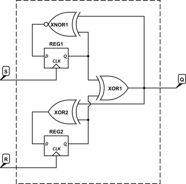
Yes, such a thing is possible, but it isn't more useful than more conventional flip-flops. Here's one way to make one:

simulate this circuit – Schematic created using CircuitLab
The output is the XOR of two internal flip-flops. If they're different, the output is high; otherwise, the output is low.
REG1 will toggle on the rising edge of the S input only if the output is low; if the output is high, it won't change state.
Similarly, REG2 will toggle on the rising edge of the R input only if the output is high; if the output is low, it won't change state.
Note that there's a requirement that near-simultaneous rising edges on both S and R have a minimum spacing, basically determined by the delay time of the feedback gates.
-
\$\begingroup\$ One limitation of this approach is that if either latch is in a metastable state when an edge arrives, the output may assume an unexpected state even though the edge should force the output into a known state. There are other ways to design the flop that would avoid that particular problem, but I know of no approach with synchronous-only flops that works in all cases where it "should" but doesn't rely upon circuit elements with known minimum propagation delays. \$\endgroup\$– supercatCommented Oct 30, 2013 at 21:29
-
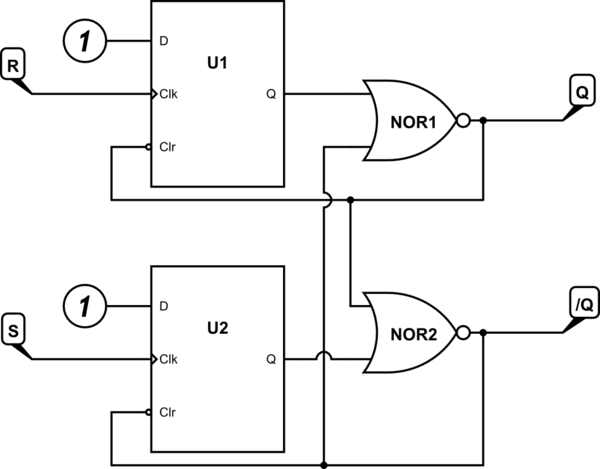
\$\begingroup\$ A practical approach if one is using async-reset flops is to put flops on the R and S lines whose data inputs is high, and whose reset input are controlled by the Q and /Q outputs of an RS latch which is operated by their outputs. In theory, this could also run into trouble if the RS latch goes metastable and prevents either flop from clocking a "high", but in practice one could adjust logic thresholds so as to avoid that difficulty (only reset a flop if Q or /Q is at a level which is guaranteed stable). \$\endgroup\$– supercatCommented Oct 30, 2013 at 21:42
-
\$\begingroup\$ @supercat: Re your first comment: The only way REG1 or REG2 could be metastable would be if you're trying to toggle them faster than the implementation technology allows, creating a setup time violation. This is what I was alluding to in my final note. \$\endgroup\$ Commented Oct 30, 2013 at 21:53
-
\$\begingroup\$ @supercat: Re your second comment: You should probably write this up as a separate answer with a diagram; I can't follow your description from the text alone. \$\endgroup\$ Commented Oct 30, 2013 at 21:56
-
\$\begingroup\$ With a normal flop, a setup/hold violation may result in a metastable condition but the next valid clock will always yield proper behavior even if the device is in a metastable state when it arrives. With the indicated circuit, that may not always be the case. \$\endgroup\$– supercatCommented Oct 30, 2013 at 22:20
In this realization, the flops should be designed so that the reset inputs will do nothing unless their logic levels suggest that the following dual-NOR latch is not in a metastable state (it's possible that depending upon the timing of input pulses to the latch, the clr input might perceive a runt pulse which would try to put one of the flops into a metastable state, but that could only happen if the other flop was cleanly high).

simulate this circuit – Schematic created using CircuitLab
This design inherently relies upon non-negative propagation delays with the flops' asynchronous reset inputs, but that isn't generally a problem. A 74HC4066 PLL chip uses something a little bit like this, except that the flops feed a single gate rather than a latch, so that there are three states: If Input 1 was hit two or more times since the last Input 2 pulse, Flop 1 will be high. If Input 2 was hit two or more times since the last Input 1 pulse, Flop 2 will be high. If the last two pulses arrived on different inputs, neither flop will be high.
When you say edge triggered it sort of implies a clock edge. People are seeing this and forcing a clock signal somehow. But in your description you just describe two inputs which are triggered on the rising edge and ignore falling edges.
This is a similar situation to MS-CMOS, where the capture latches are implemented using SR. In MS-CMOS, it is always guaranteed that ONE of the S or R signals will rise and fall; and the other will not. So an SR latch suffices.
You also did not constrain whether after one signal rises, it will fall before the next. I will assume that this is not the case, and that if Signal1 rises and sets output to 1, and before Signal1 falls, Signal2 rises; that it should set the output to 0.
I believe you are looking for a SR NOR latch, modified to toggle in the S=R=1 state. This is often called a JK latch.
Lets call J = S1 = "one input would, on rising edge, set the output to 1"
Lets call K = S2 = "and the other input would, on rising edge, set the output to 0"
Both J and R = 0 to begin. Output state is indeterminate.
Then, J rises. This sets Q = 1.
Next, J falls. The output stays 1.
Next, K rises. The output is set to 0.
Next, K falls. The output stays 0.
Next, J rises. The output is set to 1.
Next, K rises. The output is set to 0. (this is JK toggle state, if this won't happen just use NOR SR latch)
Next, J falls. The output stays 0.
Next, K falls. The output stays 0.
...
Is this what you are looking for? Wiki link, showing truth table, gate level schematic
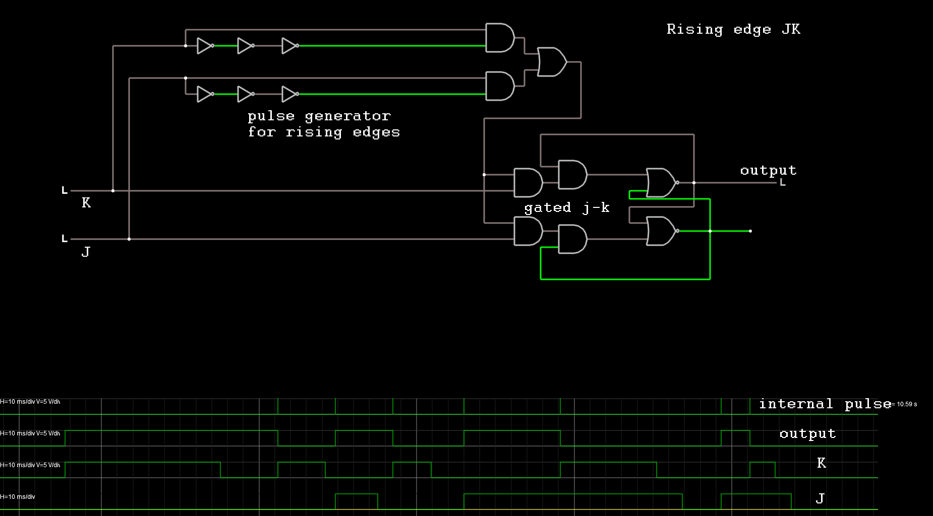
EDIT: Added fix for both inputs @ 1 simultaneously.
If you want both edges at once to toggle, generate a pulse to clock the flip flop. The pulse duration needs to be wide enough to toggle once but not twice. 1 or 3 inverters should work; I chose 3 in this case. The simple simulator didn't have 3 input ANDs so I just chained two 2-inputs back to back; either will work.
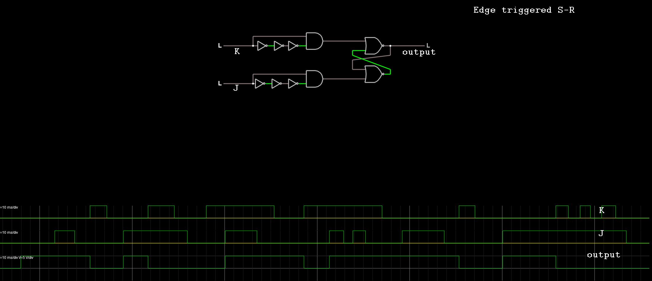
Edit2: Dave Tweed pointed out that holding one input high and repeatedly pulsing the other would toggle each time. Also he suggested combining SR with the pulse detectors. I have attached schematic and simulation below.
It is quite lean and low power/small (only 10 gates).
It will have indeterminate state if both inputs rise simultaneously (within the pulse width duration). Other implementations will have a similar effect to lesser or greater degree depending on the topology.
-
\$\begingroup\$ Your description of what happens in a JK latch when both inputs are high is incorrect. The output does not just change state once -- instead, it oscillates freely at a rate determined by the gate delays.This is not what the OP is looking for. \$\endgroup\$ Commented Jul 13, 2016 at 11:11
-
\$\begingroup\$ Thank you for the correction. I have modified the circuit to operate as intended. \$\endgroup\$– jbord39Commented Jul 13, 2016 at 12:59
-
\$\begingroup\$ This is getting silly. If you have edge detectors, why do you need the J-K logic at all? Just apply the outputs of the edge detectors directly to the R-S inputs. In fact, the circuit you show will fail if either input is held high and the other one is repeatedly pulsed -- the output will toggle on each pulse rather than remaining in the correct state. \$\endgroup\$ Commented Jul 13, 2016 at 13:05
-
\$\begingroup\$ Ah yes it is silly but we are getting closer? Thank you for the input, I have included another edit with just the rising edge detectors into the SR. This, though, requires that the pulses do not rise too closely in time to each other; or there is an invalid state. This minimum width is set by the width of the edge detectors. \$\endgroup\$– jbord39Commented Jul 13, 2016 at 13:16
-
\$\begingroup\$ So now your solution is essentially identical to the one posted by supercat almost 3 years ago. The only difference is that he uses feedback from the output of the SR latch to insure that the pulses at the outputs of his edge detectors are long enough to guarantee correct operation. Your strings of inverters offer no such guarantee. \$\endgroup\$ Commented Jul 13, 2016 at 13:29
Simpler...I'll have to desribe rather than draw...
2 dtypes one exor gate.
xor:
op = overall o/p.
xor ips = both d type q's.
dtype1:
ck = set ip.
d = dtype 2 not q.
dtype2:
ck = reset ip.
d = dtype1 q.
clock d1 (set), q's become different, xor=1.
clock d2 (reset) q's become same, xor=0.
-
1
Yes, it is called an SR latch: See google's results
If you want to read more, hyperphysics has a good explanation here which transitions to clocked flip-flops here.
Remember -- a FF is not a latch :>
-
1\$\begingroup\$ But the information you've linked to is for level-sensitive SR latches, not edge-triggered. \$\endgroup\$ Commented Oct 30, 2013 at 19:57
-
\$\begingroup\$ I see my error and the shortcomings of the invalid state. Thank you for pointing that out. I now understand the differences between an SR latch and the circuit you drew. \$\endgroup\$– HL-SDKCommented Oct 31, 2013 at 13:54
Have a look at the Wikipedia entry for the 555 timer. In bistable mode, it mentions a similar required action, although neg edge triggered and levels do interfere but one or both inputs can be capacitively coupled to keep the inputs as a pulse. Worked for me after some fiddling.
-
1\$\begingroup\$ Welcome to EE.SE. Please know you replied to a 6y old question which already had 4 answers, some of them quite good. You suggest a solution which is not very modern, when suggesting the use of a neolithic IC. \$\endgroup\$– AriserCommented Apr 18, 2020 at 12:57


