0
\$\begingroup\$

I want to design a 4-bit PISO shift register with 4 DFFs and 3 AND gates. I have gone so far that these two designs can be implemented, but I can't go further minimizing it so as to use 3 AND gates for the implementation.

If there is anyone having any suggestions I would appreciate it.
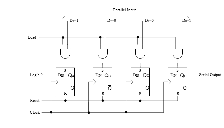
Design 1

Design 2

I have thought of another design but I didn't put it here because I think it limits the use of the shift register. Also I think that the second design is not right.

I think that there is another way to be implemented but I am not sure.
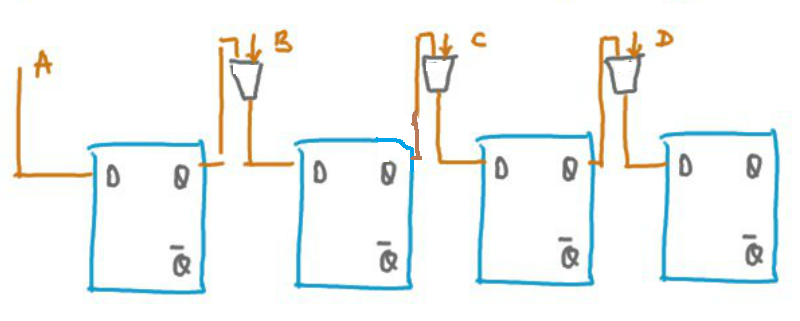
Design 3

\$\endgroup\$
10
  • \$\begingroup\$ While not providing an answer, look at Wikipedia - Shift Register under PISO. It should give you a hint. \$\endgroup\$
    – Tut
    Commented Nov 25, 2014 at 21:03
  • \$\begingroup\$ can you explain more , that design is much more complicated than my own designs. I can't take the hint. \$\endgroup\$
    – Freelancer
    Commented Nov 25, 2014 at 21:10
  • \$\begingroup\$ Last hint: Look at where the gates are used. You will need to be creative with the load control. \$\endgroup\$
    – Tut
    Commented Nov 25, 2014 at 21:12
  • \$\begingroup\$ I have implemented another design that is using the clock pulse of the circuit but I think it is wrong to put logical gates in the way of the clock pulse. \$\endgroup\$
    – Freelancer
    Commented Nov 25, 2014 at 21:13
  • \$\begingroup\$ Are you mentioning the second design? if so those logical '1' being use are the Load.but I haven't written clearly. Do you mean by some change in the first design I will be getting the answer? \$\endgroup\$
    – Freelancer
    Commented Nov 25, 2014 at 21:18

2 Answers 2

2
\$\begingroup\$

What you are doing is not what is usually referred to as a PISO.

The standard PISO has a mode input, and the shift or load function occurs on a clock.

What you're doing is rather exotic. Note that what you call a "Load" is actually two separate operations. First you have to issue a reset pulse. Then you have to issue a load pulse.

The wiki designs are indeed, as you say, more complicated than your own designs, but that's what it takes to do the job.

So the short answer is, no. You can't do what you want with 3 and gates.

\$\endgroup\$
2
\$\begingroup\$

One approach to parallel-to-serial conversion which can be useful if the parallel data input will remain valid during shifting is to use a shift register to generate a one-hot "use this bit" signal, and then "AND" each shift register output with one bit of of the parallel data input. Such an approach was used in the playfield graphic generator circuit of the Atari 2600 Video Computer System. In your particular usage case, it would require four AND gates and a four-input OR gate, but that's less extra circuitry than would be required for a more "typical" PISO when using latches that don't have asynchronous jamming inputs.

Otherwise, if you were to eliminate the leftmost "AND" gate, then provided that the first data input doesn't change between the time "RESET" goes away and the time the first clock pulse arrives, it would correctly shift out the four data bits. It would not shift out a clean "0" after that, however; I'm not sure if that's a requirement.

\$\endgroup\$

Your Answer

By clicking “Post Your Answer”, you agree to our terms of service and acknowledge you have read our privacy policy.

Not the answer you're looking for? Browse other questions tagged or ask your own question.