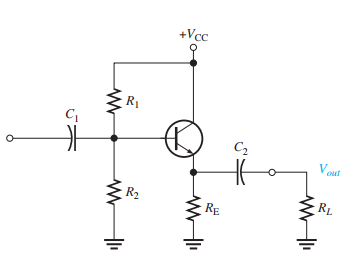
For the DC biasing of a common collector BJT amplifier, how to choose \$ R_e\$ to get a proper DC biasing? (see image attached).
Furthermore, is it possible to control \$V_{ce}\$? I am confused. Thanks!
For the DC biasing of a common collector BJT amplifier, how to choose \$ R_e\$ to get a proper DC biasing? (see image attached).
Furthermore, is it possible to control \$V_{ce}\$? I am confused. Thanks!
The chosen value for RE depends on the value of RL.
If RE is too big compared to the value of RL then, when Vout swings negative, at some signal amplitude the current through RL will equal the current through RE. This will reduce the current in the transistor's emitter to zero mA and negative clipping of the load voltage will occur.
So you need to ensure that RE is small enough compared to RL (taking into account the maximum required signal amplitude). This may mean some significant emitter current if RL has a fairly low value which will mean a fairly small value for R1 which is required to set the base bias high enough given that the emitter current and therefore the base current are larger as a result of the smaller RE. Unfortunately lowering the value of R1 will reduce the input impedence of the stage with a possible reduction of gain when the output impedence of the preceding stage is taken into account.
I would add a simple intuitive explanation to the detailed explanations in the links provided. It is based on seeing well-known electrical building blocks in this electronic circuit.
With a little more imagination, we can see two cascaded voltage dividers here:
1. High-resistance voltage divider made by R1 and R2. It is a static voltage divider with a constant ratio.
2. Low-resistance voltage divider made by the variable resistor RCE (the collector-emitter part of the transistor) and RE. It is a dynamic voltage divider with a varying transfer ratio controlled by the output voltage of the previous voltage divider.
With even more imagination, we can see that the two voltage dividers form a balanced bridge circuit. The transistor input (base-emitter junction) is connected to the bridge output... and it controls the collector-emitter "resistance" RCE in accordance to the negative feedback principle, so that to keep an almost zero voltage difference.
As a result of this connection, the output of the second voltage divider follows the output of the first one. And since it has low-resistance, it can be considered as a voltage buffer of the weak R1-R2 divider; so it can supply a load with relatively low resistance RL. Thus the whole amplifying stage can be considered as a buffered voltage divider.
See also my answer to a related question.
The lower the resistance of the buffer divider, the lower the load resistance can be. This requires RE << RL ... which in turn increases the quiescent collector current (losses). So the problem is the static RE resistance.
The happy idea that can come to us is to make RE dynamic too (to change its resistance in the opposite direction to RCE)... thus obtaining a fully dynamic divider. This is the idea behind complementary followers where the emitter resistor is replaced by another (PNP) transistor.
This is a classical emitter follower. The base voltage is set by Vcc*R2/(R1+R2). Due to the negative feedback loop, the emitter voltage "follows" the base, but with a diode drop. This in turn determines the voltage across RE (call it Vout_int), the DC value of which determines the NPN's bias current. It also determines Vce, since Vce = Vcc - Vout_int.