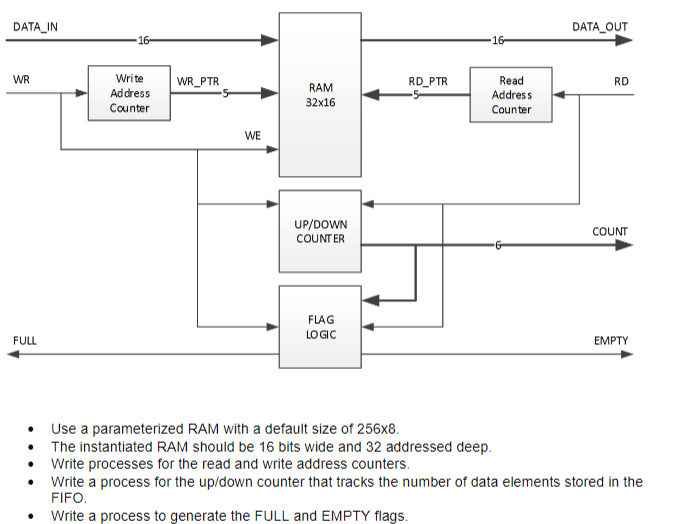
I've been tasked with designing a FIFO in VHDL for the block diagram below. I understand the general mechanism of how a simple FIFO works, but I've been struggling with how to connect the address from the read/write address counter to the address of my RAM component. I tried setting the ram address to the counter address during a read/write operation but ran into issues with the address going into an undetermined state after a write during the simulation.
Some of the code was adapted from sections of FPGA prototyping by Example by Pong P. Chu. I can link to a PDF but am not sure if that's allowed here.
Any input or suggestions would be greatly appreciated! I think most of the functionality is there though I'm sure there is still something I'm missing. Mainly I'm struggling with how to set the address for the RAM. I mapped the address input from the RAM component to a signal and then tried to write to that signal to set the address during the read/write operation but the address went to an undetermined state.
library ieee;
use ieee.std_logic_1164.all;
use ieee.std_logic_unsigned.all;
use ieee.numeric_std.all;

entity HW7 is
       port (
        wr : in  std_logic;
        rd : in  std_logic;
        main_clk : in std_logic;
        data_in    : in  std_logic_vector(15 downto 0);

        full : out std_logic;
        empty : out std_logic;
        data_out    : out  std_logic_vector(15 downto 0);
        fifo_count   : out std_logic_vector(5 downto 0)
    );
end HW7;


architecture behavioral of HW7 is

component ram_example
    generic (
        DATA_BITS: integer := 8;
        ADDR_BITS: integer := 8
    );
    port (
        clk     : in  std_logic;
        address : in  std_logic_vector(ADDR_BITS-1 downto 0);
        we      : in  std_logic;
        re      : in  std_logic;
        din     : in  std_logic_vector(DATA_BITS-1 downto 0);
        dout    : out std_logic_vector(DATA_BITS-1 downto 0)
    );
end component;

component genericCounter
    generic(
    upDownCounterSize : integer := 16
    );
    port(
    clk_a : in std_logic := '0';
    clr : in std_logic := '0';
    upInput : in std_logic := '0';
    downInput : in std_logic := '0';

    count : out std_logic_vector(upDownCounterSize - 1 downto 0) := (others => '0')
    );
end component;

signal wr_addr,wr_addr_next,wr_addr_succ : std_logic_vector(4 downto 0) := (others => '0');
signal rd_addr,rd_addr_next,rd_addr_succ : std_logic_vector(4 downto 0) := (others => '0');
signal ram_address : std_logic_vector(4 downto 0) := (others => '0');
signal cnt_signal : std_logic_vector(5 downto 0) := (others => '0');
signal dataIn : std_logic_vector(15 downto 0) := (others => '0');
signal dataOut : std_logic_vector(15 downto 0) := (others => '0');
signal full_flag,full_next : std_logic := '0';
signal empty_flag,empty_next : std_logic := '0';
signal mode : std_logic_vector(1 downto 0);

begin

myRam : ram_example generic map(
    DATA_BITS => 16,
    ADDR_BITS => 5
    )
    port map(
    clk => main_clk,
    address => ram_address,
    we => wr,
    re => rd,
    din => dataIn,
    dout => dataOut
    );

myCounter : genericCounter generic map(
    upDownCounterSize => 6
    )
    port map(
    clk_a => main_clk,
    upInput => wr,
    downInput => rd,

    count => cnt_signal
    );


process(main_clk)
begin

if( rising_edge(main_clk) ) then
    wr_addr <= wr_addr_next;    --set the addresses and flags to the next state
    rd_addr <= rd_addr_next;
    full_flag <= full_next;
    empty_flag <= empty_next;
end if;
end process;

wr_addr_succ <= std_logic_vector(unsigned(wr_addr) + 1);
rd_addr_succ <=  std_logic_vector(unsigned(rd_addr) + 1);

mode <= wr & rd;

process(wr_addr,wr_addr_succ,rd_addr,rd_addr_succ,mode,full_flag,empty_flag)
begin

wr_addr_next <= wr_addr;    --set the next address registers to the current register so we stay in the same place until a read or write signal occurs.
rd_addr_next <= rd_addr;
full_next <= full_flag;
empty_next <= empty_flag;

case mode is
    when "00" => --do nothing
    when "01" => --read
        if(empty_flag /= '1') then  -- if FIFO isn't empty, increment the read address by 1
            rd_addr <= rd_addr_succ;
            full_next <= '0';
            if(rd_addr_succ = wr_addr) then -- if we read and the read address + 1 equals the write address, set the empty next flag
                empty_next <= '1';
            end if;
        end if;
    when "10" => --write    -- if FIFO isn't full, increment the write address by 1
        if(full_flag /= '1') then
            wr_addr <= wr_addr_succ;

            empty_next <= '0';
            if(wr_addr_succ = rd_addr) then -- if we write and the write address + 1 equals the read address, set the full next flag
                full_next <= '1';
            end if;
        end if;
    when others => --read and write
        wr_addr_next <= wr_addr_succ;
        rd_addr_next <= rd_addr_succ;
end case;
end process;


full <= full_flag;
empty <= empty_flag;
dataIn <= data_in;
data_out <= dataOut;
fifo_count <= cnt_signal;
end behavioral;
----------------------------------------------------------------------
library ieee;
use ieee.std_logic_1164.all;
use ieee.std_logic_unsigned.all;  -- Required for type conversions

entity ram_example is
    generic (
        DATA_BITS: integer := 8;
        ADDR_BITS: integer := 10
    );
    port (
        clk     : in  std_logic;
        address : in  std_logic_vector(ADDR_BITS-1 downto 0);
        we      : in  std_logic;
        re      : in  std_logic;
        din     : in  std_logic_vector(DATA_BITS-1 downto 0);
        dout    : out std_logic_vector(DATA_BITS-1 downto 0)
    );
end ram_example;

architecture behavioral of ram_example is

   --declaration of RAM type
   type ram_type is array (0 to 2**ADDR_BITS-1) of std_logic_vector(DATA_BITS-1 downto 0);

   --declaration of RAM
   signal ram : ram_type;

   begin

   --process for read and write operation.
   process(clk) begin
       if(rising_edge(clk)) then
           if(we='1') then
               ram(conv_integer(address)) <= din;
           end if;
           if(re='1') then
           dout <= ram(conv_integer(address));
           end if;
       end if;
   end process;

end behavioral;

