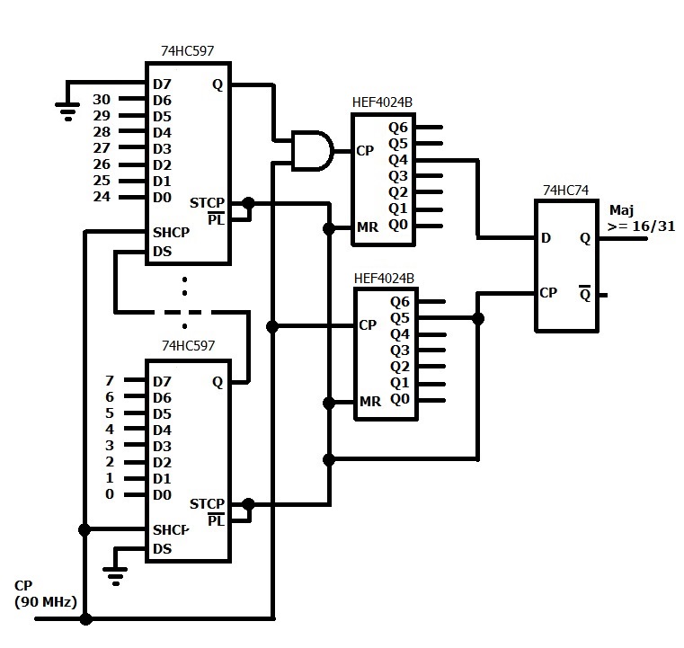
Connect the 31 inputs (0-30 in the diagram below) to four 8-bit parallel-in, serial out shift registers such as the 74HC597 which are cascaded in series (only two shown). Clock the serial output of the last register into a binary counter such as the 74HC4024. Use another 74HC4024 counter to keep track of when 32 clock pulses have occurred which then repeats the cycle.

For some crazy reason the original CD4024, and the follow-on 74HC4024 started numbering their flip-flops with Q1 instead of Q0. Very confusing. So I am showing the NXP part (HEF4024B) instead which corrected this anomaly.
So every 32 clock pulses (when Q5 of the second counter goes high), if at least 16 inputs were high (meaning Q4 of the first counter is 1), then this status is latched into a D-type flip-flop (74HC74) and remembered until the next set of 32 clock pulses complete. Meanwhile the inputs are reloaded in parallel to the shift registers.
This is somewhat of a special case, in that the majority threshold is a power of two, so only one pin (in this case Q4, representing 16-31) has to be queried. If instead the threshold was 14/27 for example, an address decoder would need to be added, to separate out the values 14 and 15 in addition to 16.
With a 90 MHz input clock, there will be a maximum of 355 ns delay from a change in the input until the update of majority status at the output.
Note -- not all "glue logic" necessarily shown, but this should get across the idea.


