0
\$\begingroup\$

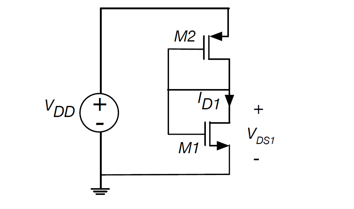
So I have a circuit shown below, that looks to me likes it's a CMOS inverter circuit. In this question, we're asked to find the current and voltage across drain-source voltage of the NMOS component.

The values given for the PMOS are as follows:
VDD = 5.003V
VT,pmos = -509mV
µpCox = 101µV/A2
W/L = 2µm/1µm
Lambda = 0V-1

Likewise for the NMOS:
VT,nmos505mV
µpCox = 209µV/A2
W/L = 9µm/1µm
Lambda = 0V-1

Here's the schematic: Aforementioned Circuit

So in my attempt to figure this out on my own, I got this:
Clearly, VS of the PMOS = 5.003V
Now after this is where I start to really question myself, and end up going in circles.If I assume that VG = VD based on the circuit diagram, then VGS and VDS are going to give the same value. Won't that then mean the PMOS is cut off?

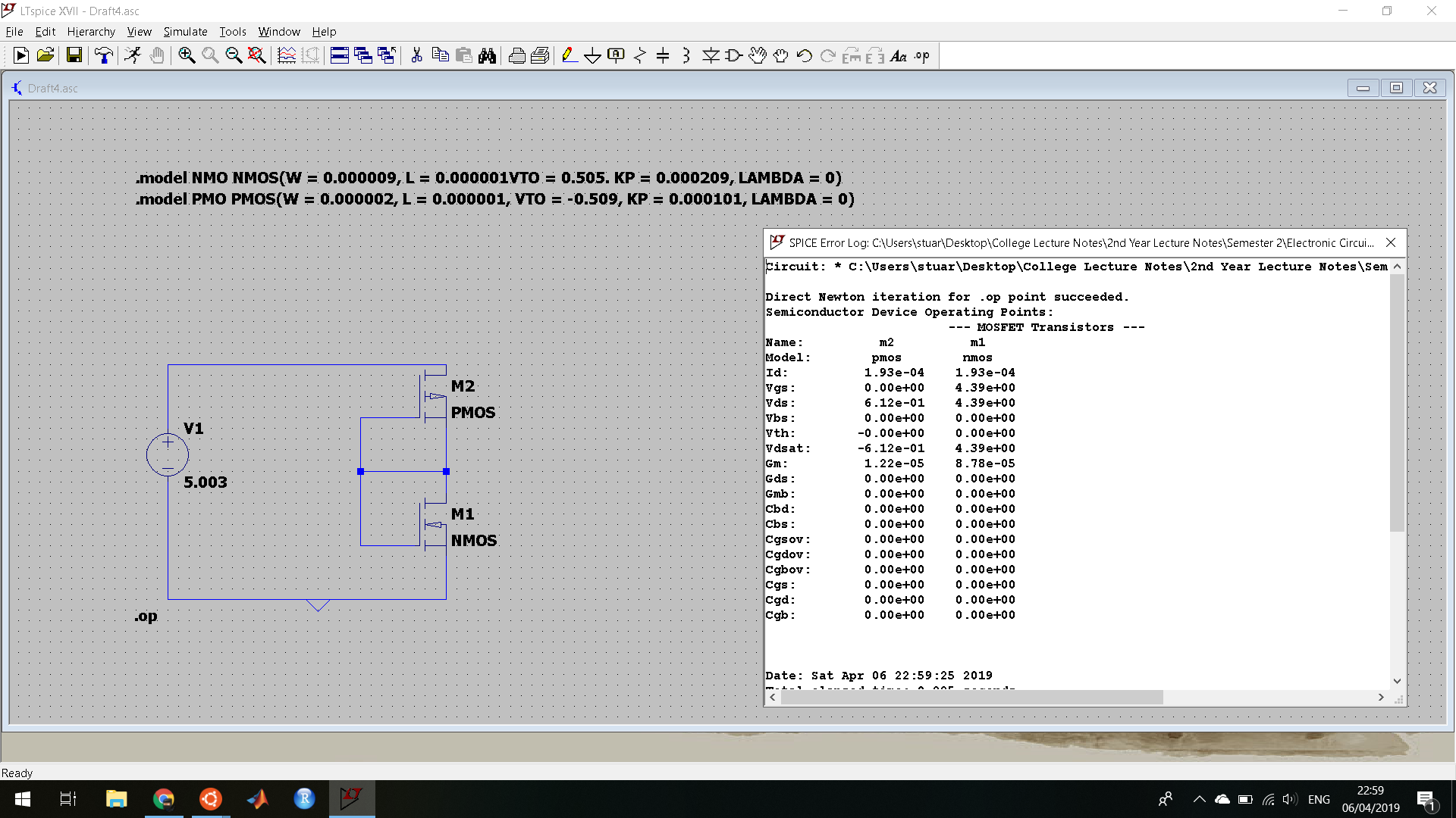
I've also simulated the circuit in LTSpice. This gives VGSDS as the same value. Which appears to approximately be the source voltage minus the threshold voltage, but a little different. Here's that diagram and the related info it obtains.

LTSPICE Output and schematic

Any help is appreciated. Especially in any conceptional mistakes or general assumption methods for the future!

\$\endgroup\$
7
  • 4
    \$\begingroup\$ Your PMOS in the simulation is connected backward. \$\endgroup\$
    – G36
    Commented Apr 6, 2019 at 22:19
  • \$\begingroup\$ Wait really? What way should I have it hooked up? \$\endgroup\$ Commented Apr 7, 2019 at 17:33
  • \$\begingroup\$ Notice the arrow symbol on a PMOS and compare it with your schematic and LTSpice. \$\endgroup\$
    – G36
    Commented Apr 7, 2019 at 17:44
  • 1
    \$\begingroup\$ You dont change the arrow only, you flip the whole symbol. \$\endgroup\$
    – Linkyyy
    Commented Apr 8, 2019 at 8:41
  • 1
    \$\begingroup\$ Move->Ctrl-R, Ctrl-R, Ctrl-E flips the symbol vertically. \$\endgroup\$ Commented Jul 13, 2020 at 4:20

2 Answers 2

1
\$\begingroup\$

Like any other analog circuit, you should try to deal with these problems as if it is a big puzzle of voltages and currents. You kind of need to solve them simultaneously, and the "shapes of the puzzle pieces" are the voltage-current equations of each circuit component.

In this case, when looking at the currents flowing through the circuit, you can notice that the gates do not draw any current, so the current only flows from M2 source -> M2 drain -> M1 drain -> M1 source and back up through V1 (currents always flow in loops). The important part is that it is the same through M1 and M2.

We know that both transistors are in saturation (\$v_{DSn} = v_{GSn}\$ and \$v_{DSp} = v_{GSp}\$), so you can use the following (simple model) equations:

$$i_{Dn,Dp} = \mu_{n,p}C_{ox}\cdot \frac{W}{2L}(v_{GS}-v_{TH})^2(1+\lambda_{n,p} v_{DS})$$

We know that \$i_{Dn} = i_{Dp}\$, and we also know that \$v_{GSn} - v_{GSp} = 5.003V\$. This should be enough information to calculate both current and voltage.

\$\endgroup\$
0
\$\begingroup\$

There is about 4 volts across the 2 FETs.

Give the current is the same, we can write

Kp * 2 * VeffectiveP^2 = Kn * 9 * VeffectiveN^2

And VeffectiveP + VeffectveN = 4

\$\endgroup\$
1
  • \$\begingroup\$ Do you understand this information? \$\endgroup\$ Commented Apr 8, 2019 at 4:46

Your Answer

By clicking “Post Your Answer”, you agree to our terms of service and acknowledge you have read our privacy policy.

Not the answer you're looking for? Browse other questions tagged or ask your own question.